Entry #007 - Jun 9th, 2026
Making a D-flip-flop from logic gates and connecting it to the 6502
I am stuck with the 6502 and cannot get it working. To generate new ideas, I rewatch Ben Eater’s video about the VIA. As we saw earlier, the reason the 6502 cannot directly drive peripherals is that the data placed on the bus is only present for a single clock cycle. We therefore need something that can capture the data. In previous videos, Ben Eater explained how to build RS and D flip-flops. These are very simple circuits that can be built with just a few logic gates and are capable of storing a value and updating it based on various signals. An RS flip-flop has a set input that activates the output and a reset input that deactivates it. A D flip-flop, on the other hand, has a data input and a clock input, and it captures the data on every rising edge of the clock. That’s exactly what we need here.
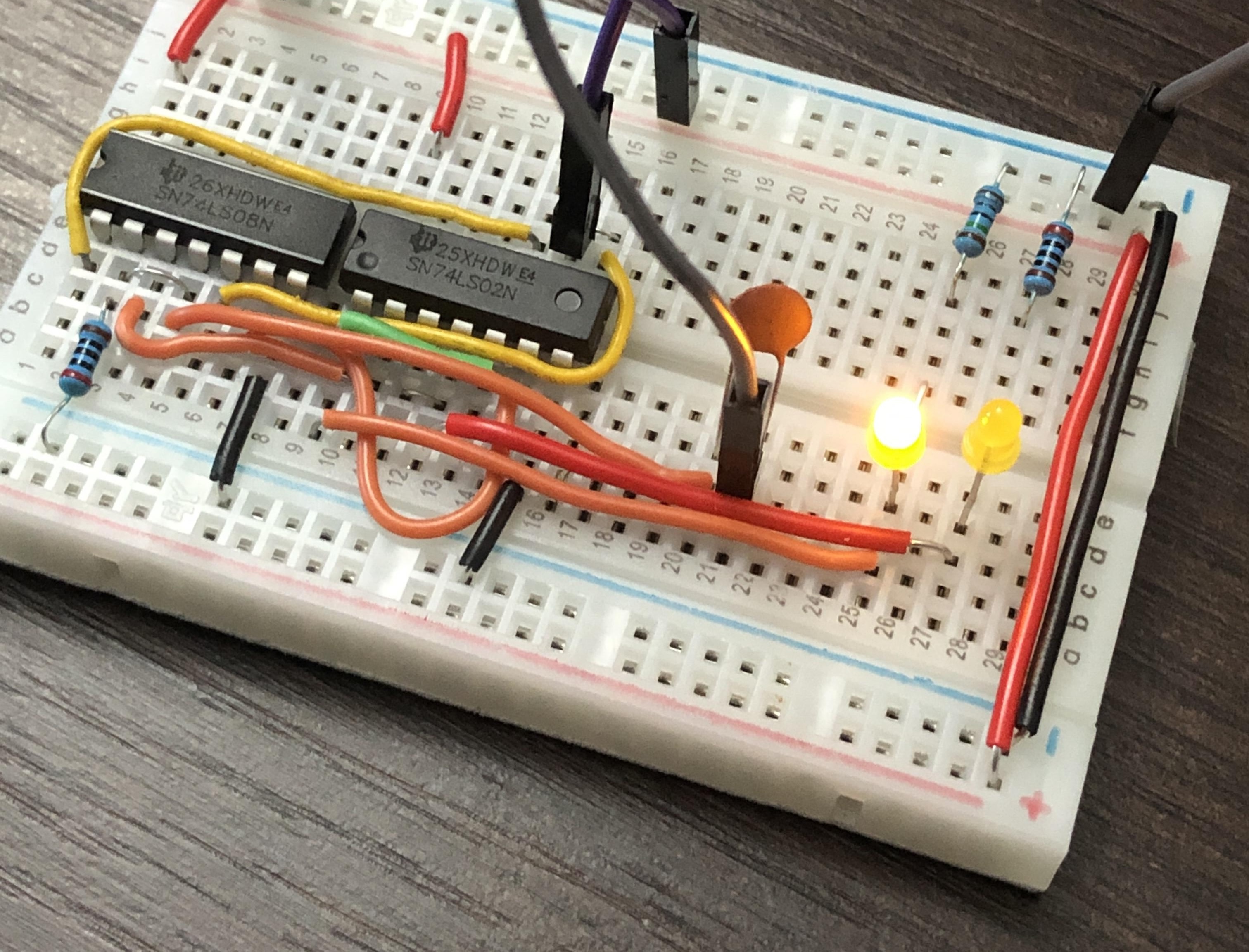
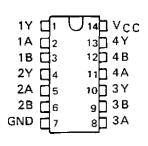
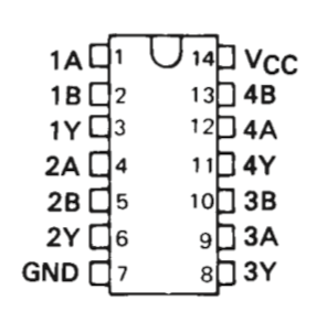
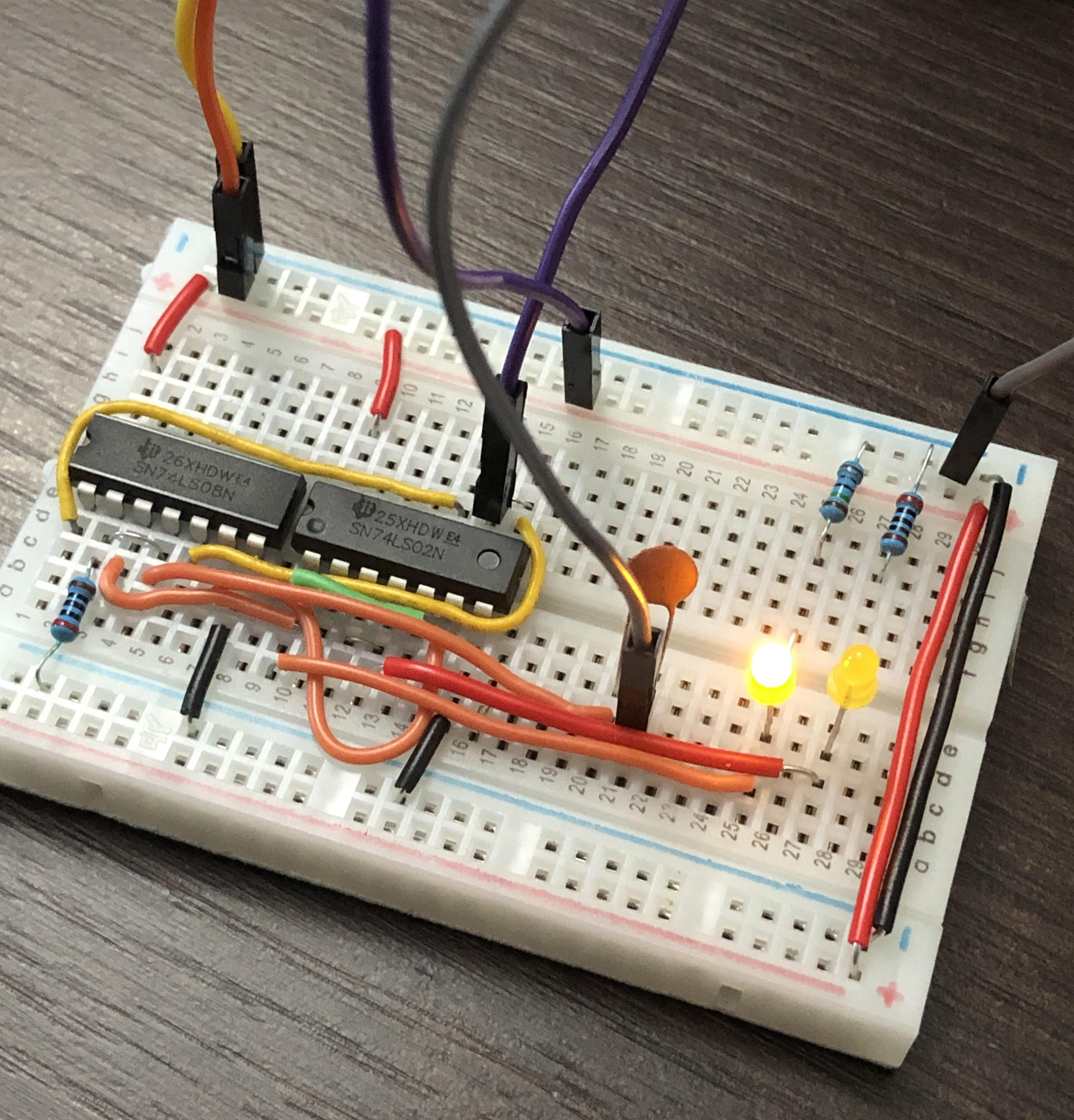
I rewatch Ben Eater’s video about the D flip-flop and implement the circuit on a new small breadboard. I use one 74LS02 and one 74LS08 chips, which contain four NOR gates and four AND gates, respectively. There are quite a few connections to make, and I need to be careful because the pins are not arranged the same way on both chips. To avoid mistakes, I sketch the circuit on paper and write down the pins that need to be connected. I also add two LEDs to visualize the state of the output (one for the normal output and one for the inverted output).
As usual, I test the circuit by manually controlling the input signals. At first it doesn’t work, but that’s because I forgot to connect the two power rails of the breadboard together —a mistake that I unfortunately do quite often. Once this is fixed, everything works perfectly: on the rising edge of the clock signal, the value present on the input is captured on the output. Changing the input signal does not affect the output as long as the clock remains unchanged. Unlike a latch, which continuously updates its output while the Enable signal is 1, a flip-flop only captures the data at the exact moment when the clock transitions from 0 to 1. I confirm that this is indeed how my circuit behaves.
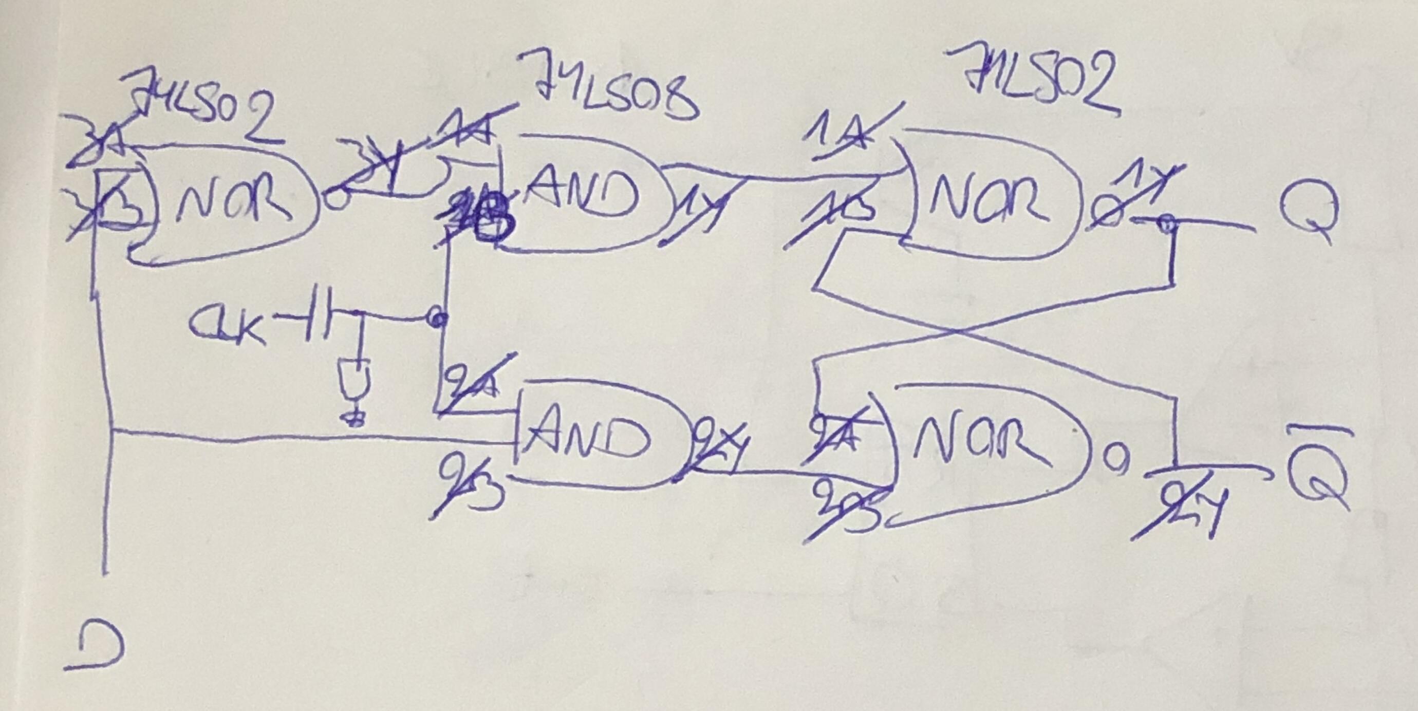
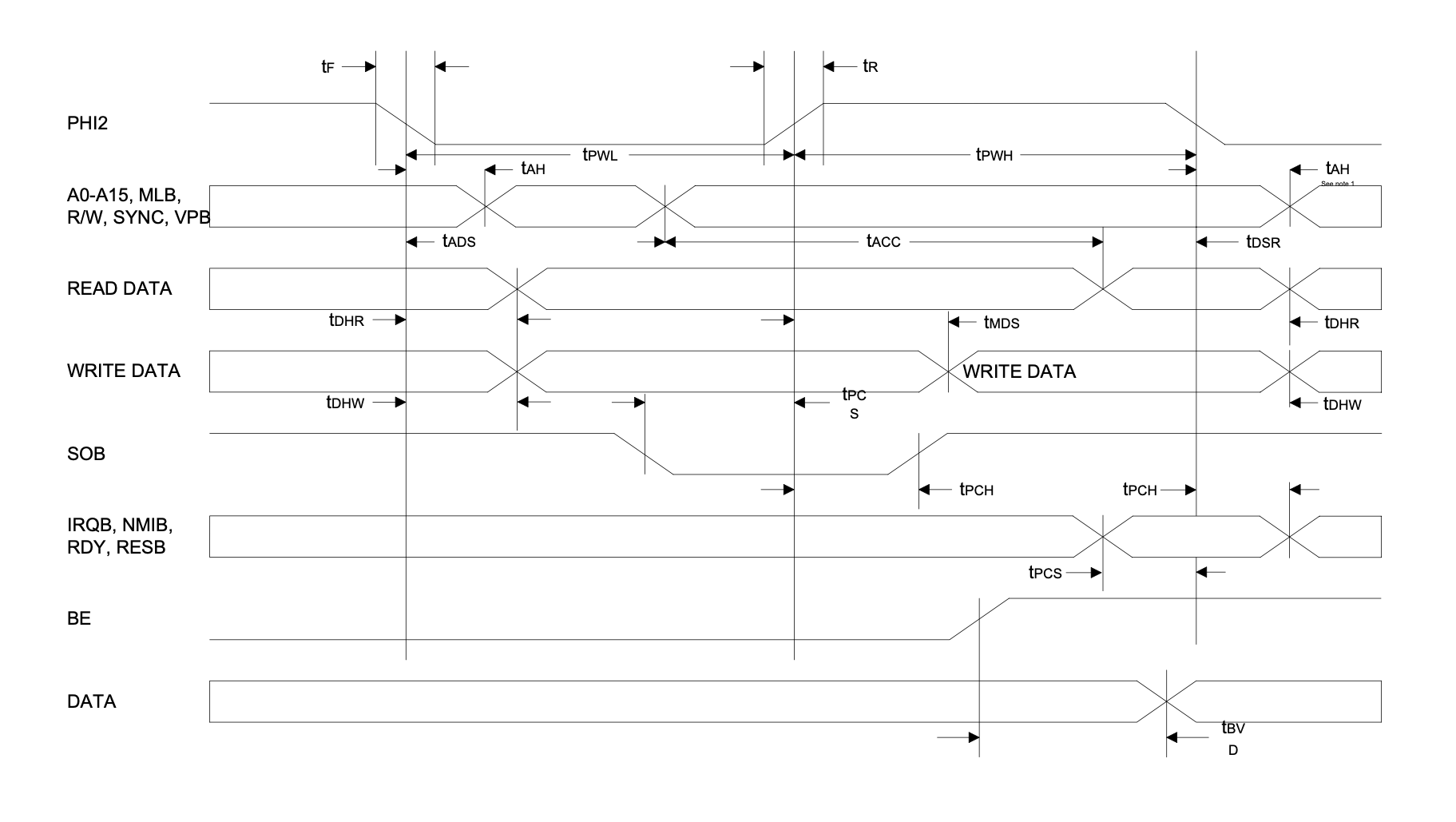
The circuit will operate as follows: the input of the flip-flop is connected to one of the eight lines of the data bus. When we want to change the state of the flip-flop, the CPU places the desired value on the data bus. The clock signal then triggers the flip-flop to capture that value. If we stop there, however, the flip-flop captures every data that appears on the bus, and the CPU has no way to prevent it. We need to add something equivalent to the Chip Select mechanism discussed earlier, meaning that we must use the address lines so that the flip-flop is only enabled when the CPU accesses an address assigned to it. Before tackling that, I first want to verify that the flip-flop works correctly with the data bus. I check the 6502 datasheet to ensure that data is present on the bus when the clock’s rising edge occurs, and that is indeed the case. So it should work.
I connect the flip-flop input to the D0 line of the 6502 and the clock input to PHI2. I review the test program that is still stored in ROM and calculate what we should observe. The result is as follows:
| Address | R/W | Data | D0 |
|---|---|---|---|
0xFFFC |
R |
00 |
0 |
0xFFFD |
R |
80 |
0 |
0x8000 |
R |
A9 FF |
1 1 |
0x8002 |
R |
8D 02 40 |
1 0 0 |
0x4002 |
W |
FF |
1 |
0x8005 |
R |
A9 02 |
1 0 |
0x8007 |
R |
8D 00 40 |
1 0 0 |
0x4000 |
W |
02 |
0 |
0x800A |
R |
A9 05 |
1 1 |
0x800C |
R |
8D 00 40 |
1 0 0 |
0x4000 |
W |
05 |
1 |
0x800F |
R |
4C 05 80 |
0 1 0 |
I power up the circuit, and I can immediately see the flip-flop changing state, which is a good sign. I reset the CPU and watch carefully. After a reset, the CPU takes seven clock cycles to initialize, so we should see the expected sequence begin seven cycles after releasing the reset button. As usual, the Arduino provides the clock signal, and we can use the fact that its LED blinks on every clock transition to follow the execution of the program. Focus is required here, but it is very rewarding to see the flip-flop changing state exactly when expected.
The flip-flop is working correctly, but for now it captures everything that goes through the bus, which is not very useful. We need to add some logic so that it only captures data intended for it. To reuse the existing program, I decide to use A15 and A14 so that the address 0x4000 can be used to talk to the flip-flop. I also take /RW into account so that the circuit only responds to write operations. In this particular case it is not strictly necessary, since the flip-flop can only receive data and never send any. The idea is to add AND gates to the flip-flop inputs so that the signal reaching it only passes when the appropriate conditions are met. My first thought is to gate the data signal itself, but I quickly realize that this is a mistake. It is the clock signal that must be gated, because it is the clock that captures the data. The input data can vary freely according to whatever is happening on the bus, but the flip-flop will only capture that data when the enabling signals are present. The rest of the time, no capture signal reaches the flip-flop.
To summarize, we want a capture to occur only when all of the following conditions are true:
A15 = 0A14 = 1/RW = 0PHI2 = 1
The capture signal should therefore be the result of the following expression:
CLK = /A15 AND A14 AND /RW AND PHI2
I did not use all of the logic gates available on the chips when building the flip-flop. There is still one NOR gate and two AND gates available, and if necessary we also have five inverters left on the chip used for the ROM’s Chip Select. Let’s see what we can do with that.
Here is the truth table of a NOR gate:
a |
b |
a NOR b |
|---|---|---|
0 |
0 |
1 |
0 |
1 |
0 |
1 |
0 |
0 |
1 |
1 |
0 |
We can see that:
a NOR b
is equivalent to:
/a AND /b
If we rearrange our expression, we can write:
CLK = (/A15 AND /RW) AND A14 AND PHI2
Using the NOR/AND equivalence, we can transform it into:
CLK = (A15 NOR RW) AND A14 AND PHI2
This uses exactly one NOR gate and two AND gates —precisely what we have available. Perfect.
I build the circuit and, before testing it, I once again review the program to determine what we should observe. This time, the flip-flop should only change state when the CPU performs a write to an address in the range 0x4000–0x7FFF, giving the following sequence:
| Address | R/W | Data | LED |
|---|---|---|---|
0xFFFC |
R |
00 |
0 |
0xFFFD |
R |
80 |
0 |
0x8000 |
R |
A9 FF |
0 0 |
0x8002 |
R |
8D 02 40 |
0 0 0 |
0x4002 |
W |
FF |
1 |
0x8005 |
R |
A9 02 |
1 1 |
0x8007 |
R |
8D 00 40 |
1 1 1 |
0x4000 |
W |
02 |
0 |
0x800A |
R |
A9 05 |
0 0 |
0x800C |
R |
8D 00 40 |
0 0 0 |
0x4000 |
W |
05 |
1 |
0x800F |
R |
4C 05 80 |
1 1 1 |
Just as before, it takes some concentration to follow the execution of the program, but it is clear that everything works as expected.
Using a D flip-flop with the 6502 was not part of the original plan, but it turned out to be very rewarding and helped me better understand what might happen inside chips that communicate over a data bus, such as ROMs or the VIA. I’m very glad I took this little detour.
What’s Next
The 6502 can now control an LED and change its state according to the logic defined by the program. This is still quite limited, of course, but it already forms a simple system that is worth emulating. Before moving on, however, I would like to make things a bit more interesting by adding the ability for a user to inject data into the system through a push button. This time, the goal is to create an input peripheral, capable of placing data onto the bus when requested by the CPU. Once that is done, I will finally be able to write interactive programs and begin working on the emulator itself.
I use generative AI to write and/or translate the content featured on this website. AI serves only as a tool for productivity and inspiration, I make sure that the final texts always reflect my personal voice and style.