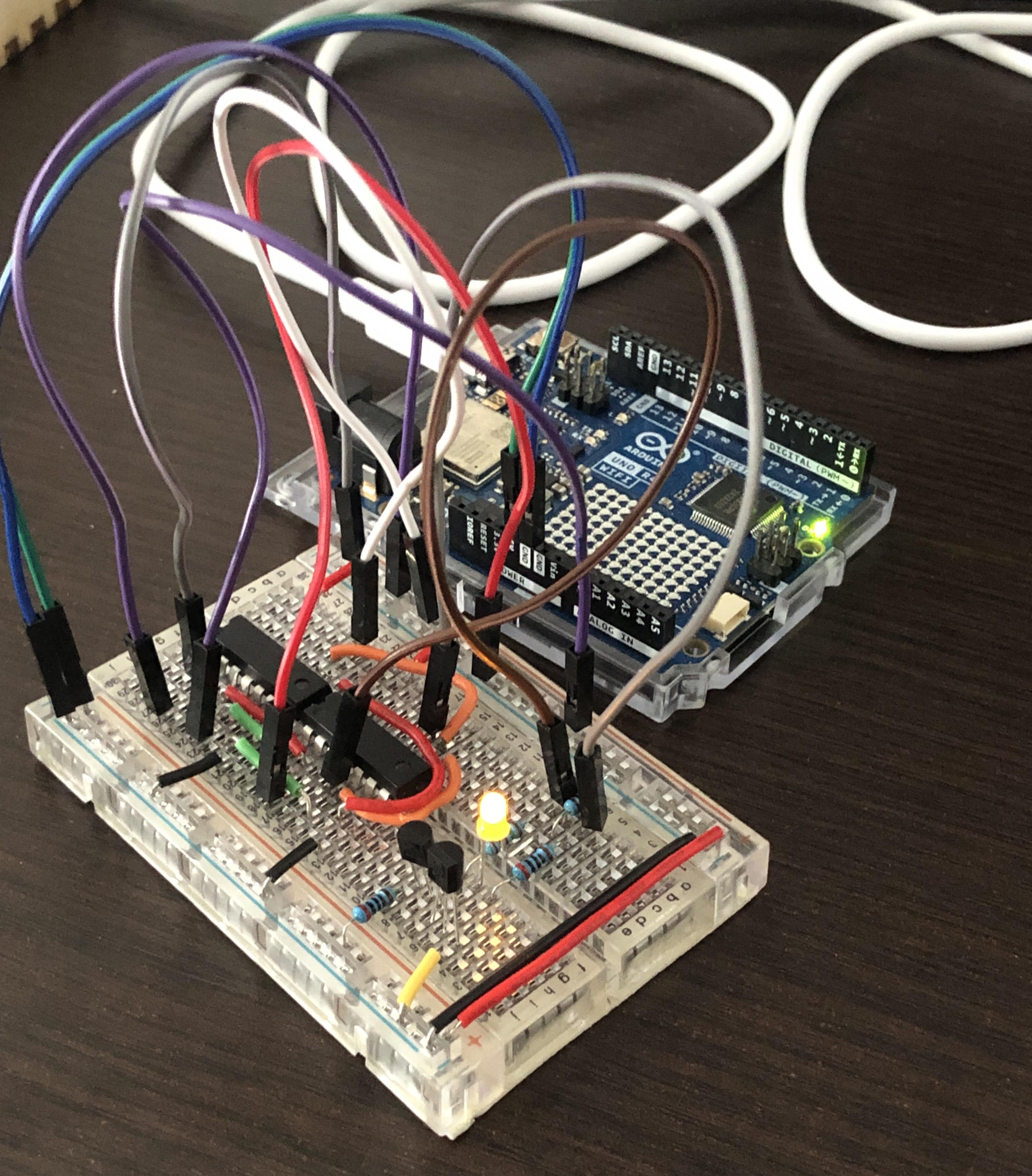
Entry #008 - Jun 13th, 2026
Making an input peripheral for the 6502
Now that the 6502 is able to drive an LED through a D latch, the next goal is to make it read an external input. That is to create a peripheral from which the CPU can read data. The idea is to connect a push button and allow the processor to read its state by issuing a read instruction to the memory address assigned to the button.
Writes to the bus and the high-impedance state
My first idea was to connect the button directly to one of the data bus lines, but that would cause problems when the CPU or other peripherals also want to write to the bus. To avoid interfering with other communications, the button must only connect to the bus when it is being read by the CPU. We didn’t have this issue with the latch because it only reads from the bus, whereas the button must be able to drive the bus.
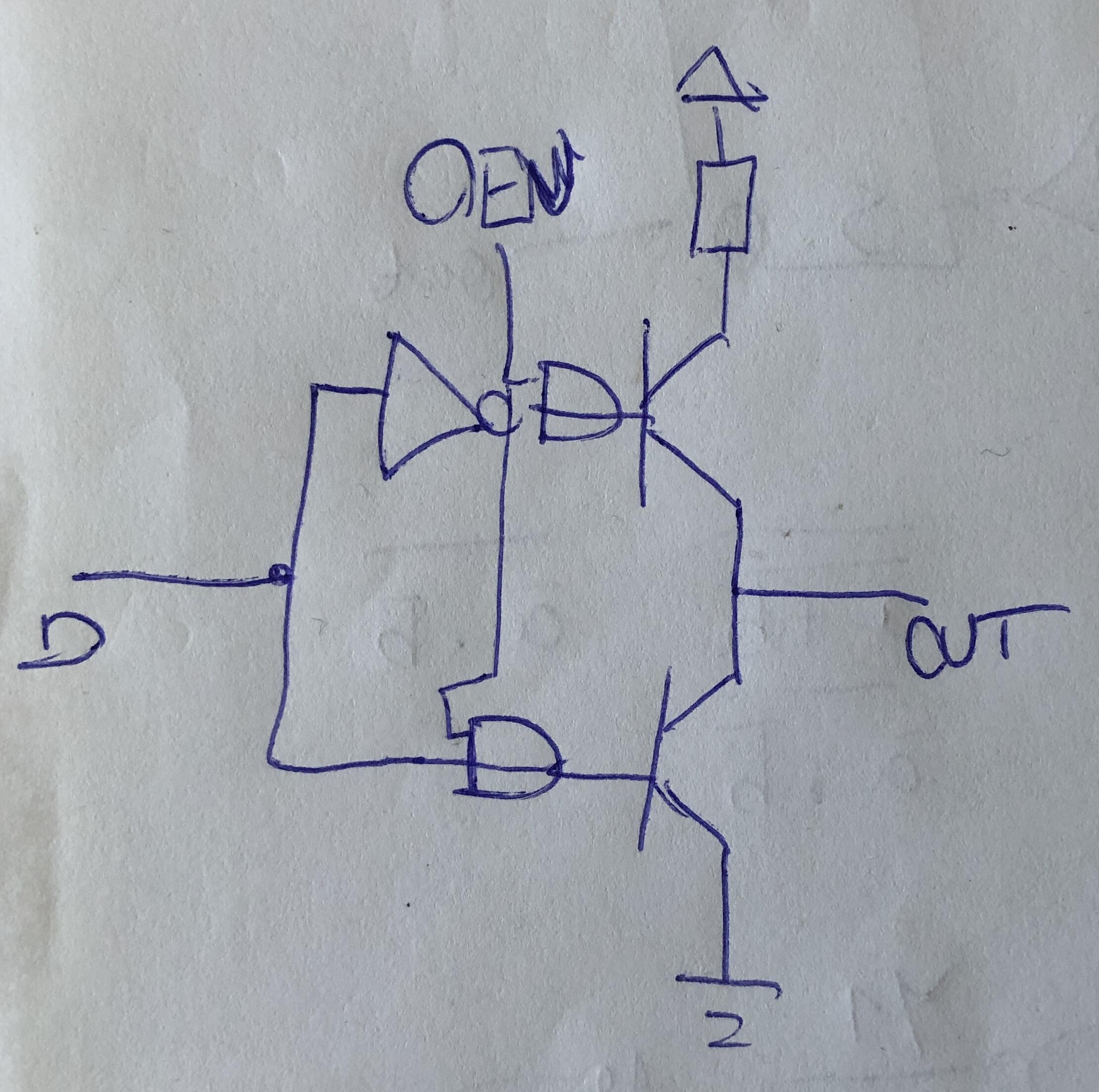
I quickly came up with the idea of using two transistors in series so that the midpoint can be connected either to +5V or to 0V. And if neither transistor is conducting, the output becomes disconnected. I’ve probably seen circuits like this many times throughout my life, and it feels like I’m reinventing an electronic output stage. It’s fascinating. The disconnected state is called the high-impedance state, and outputs capable of entering this state are known as tri-state outputs.
The transistors are driven directly by the data signal or its inverse, depending on the case. They are also enabled by a control signal. The base of each transistor is therefore connected to the output of a logic gate that combines the data signal and the control signal. This control signal corresponds to the Output Enable typically found on integrated circuits.
What about the clock?
As with the latch, a memory range must be allocated to the button. My first thought was to use the 0x0000-0x3FFF range that had remained unused so far, but that wouldn’t be a good idea because I plan to add RAM later, and it will need to cover addresses 0x0100-0x01FF for the stack.
I therefore decided to allocate the same memory range as the latch. The distinction between the two peripherals will be made using the read/write signal: the latch only responds to writes, while the button only responds to reads.
So we need an enable signal that satisfies the following conditions:
A15 = 0A14 = 1RW = 1CLK?
The clock signal raised an interesting question. For the latch, we used the clock to trigger data capture, but here, since the CPU is the one reading, does the peripheral need to do anything? Is it enough to place the data on the bus whenever the address and RW signals are valid? How can we be sure that the bus is free?
Curious, I asked ChatGPT, which told me that the peripheral should only connect to the bus during the high phase of the clock (when the signal is 1), since this is the phase during which the signals are stable, the low phase being when things are being set up. It explained that the CPU reads data near the end of the high clock phase.
ChatGPT also explained that write-addressable peripherals should sample data near the end of the high clock phase as well. That surprised me because in my D latch implementation I captured data on the rising edge of the clock—right at the beginning of the stable phase—and it seemed to work fine. ChatGPT commented: “On a real 6502, the data is typically already valid by then, but you’re leaving yourself less timing margin.”
This prompted me to take a much closer look at timing considerations.
Studying the timing
At this point I knew that on every clock cycle the CPU places an address on the address bus and exchanges a piece of data, but I didn’t know the detailed sequence of events. I decided to rewatch Ben Eater’s video in which he explains timing considerations while connecting a RAM chip. It helped me understand what actually happens during a clock cycle and how to read timing diagrams.
Looking at the documentation for the 6522, I noticed that data is indeed expected to be valid around the falling edge of the clock, and the read operation appears to occur at that moment.
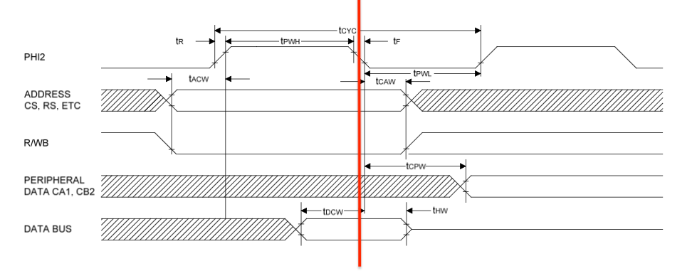
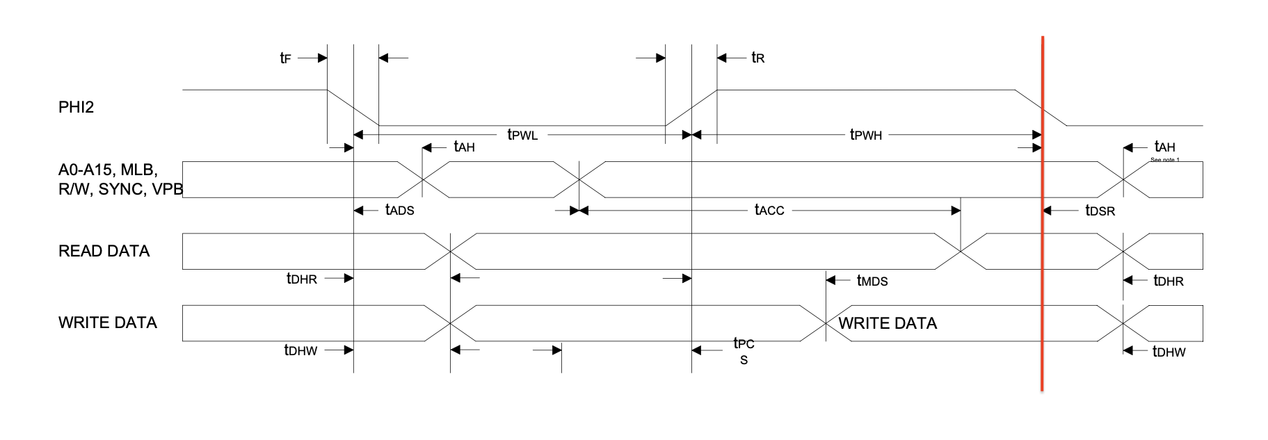
I then consulted the 6502 documentation. I had previously skimmed over the timing diagrams, but now was the time to study them carefully. I understood that for the CPU to read data reliably, that data must remain stable for a certain amount of time before and after the falling edge of the clock.
The diagram shows that the CPU keeps the address valid for a short period after the falling edge, and by looking at the timing values I noticed that this duration is always equal to the required data hold time. My conclusion was that if I keep the data on the bus as long as the address remains valid, everything should work. On the other hand, if I restrict the data to the period where the clock is high, as ChatGPT suggested, it would not be held long enough. But can we really be sure that the bus is free whenever the address is valid?
ChatGPT told me that due to propagation delays, restricting the data to the high clock phase generally works without problems and is in fact the standard approach.
I’ll come back to timing later. For now, I can continue with the implementation.
Implementing the circuit
The enable signal must then follow the equation:
CS = OE = /A15 AND A14 AND RW AND CLK
which can be rewritten as:
CS = OE = /A15 AND /(A14 NAND RW) AND CLK
Using the fact that /a AND /b is equivalent to a NOR b:
CS = OE = (A15 NOR (A14 NAND RW)) AND CLK
And finally, replacing the final AND with a NAND so that only two gate types are needed, which inverts the output signal:
/CS = /OE = (A15 NOR (A14 NAND RW)) NAND CLK
The upper transistor must be active when the data is 1, and the lower transistor when the data is 0. We therefore need at least one inversion of the data signal. Since the transistors are only active when CS or OE are 1, we have:
Th = D AND CS
Tl = /D AND CS
Using the NOR equivalent again:
Th = /D NOR /CS
Tl = D NOR /CS
That gives us a total of 2 NAND gates and 3 NOR gates. The chips contain four of each, so we’re good.
I started by implementing the logic and planned to add the transistors afterward. Before wiring everything, I drew the schematic, chose which gates from which chips would be used, and displayed the pinouts on my screen. Everything went smoothly until I realized I’d forgotten to account for the inversion required for the upper transistor. I used one of the spare NAND gates for that.
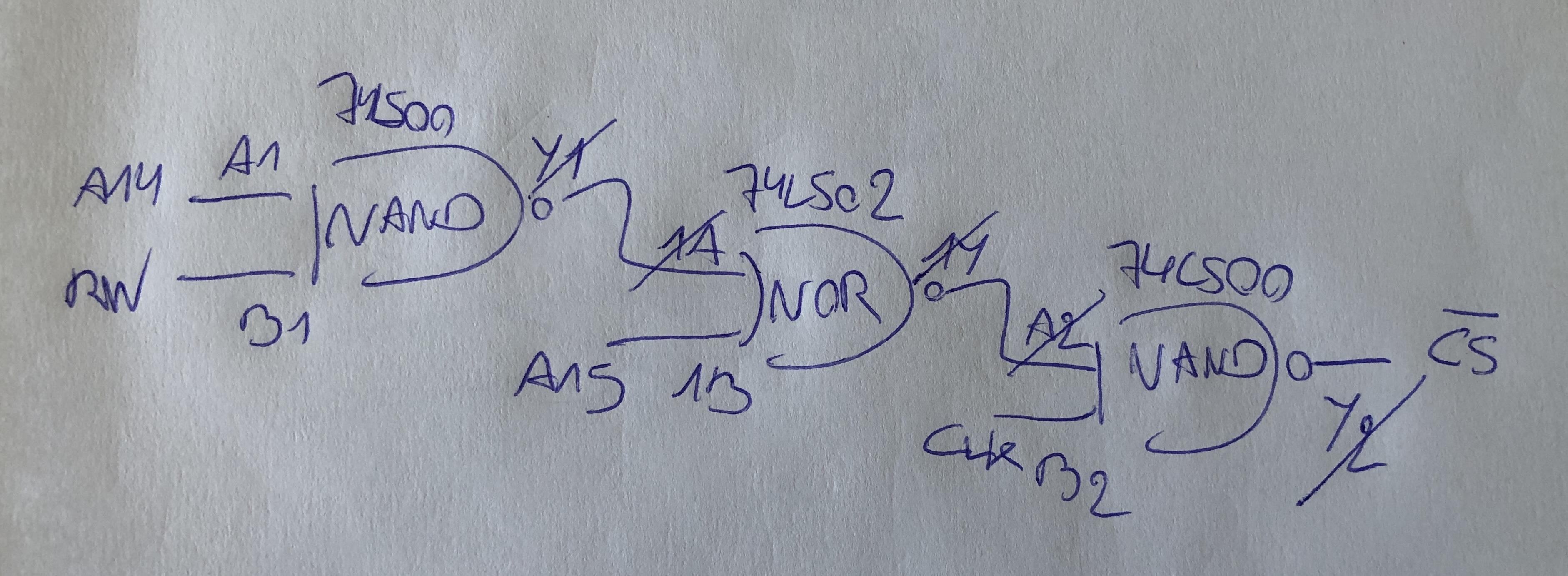
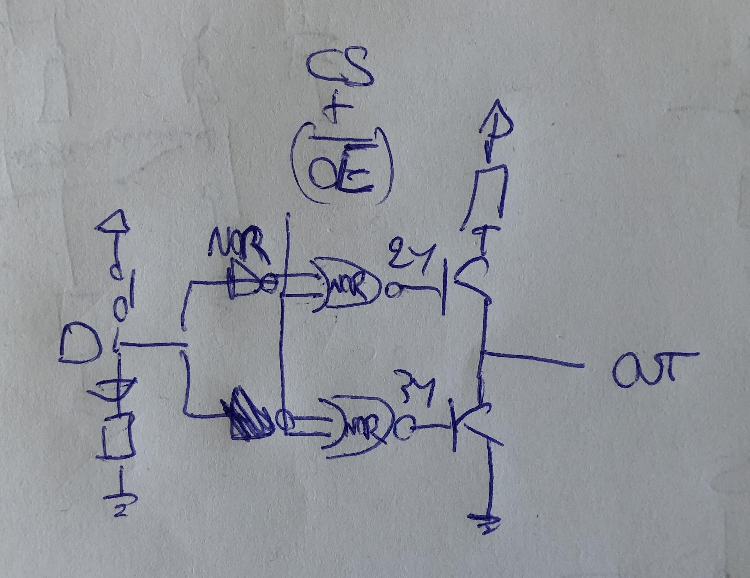
As usual, I started by testing everything manually. I connected all the signals so that Chip Select was active and forced the data signal to 1. When I powered the circuit, the upper transistor control signal turned on. A good sign.
I played with the signals and confirmed that everything behaved as expected. When the data is 1, the upper transistor is active. When the data is 0, the lower transistor is active. And when the enable conditions are not met, neither transistor is active.
For the transistors I used P2N2222A devices. I wondered whether I should place a resistor on the base. That depends on whether the outputs of the logic chips already include current limiting resistors. Since LEDs behave normally when connected through external resistors, I assumed they don’t. ChatGPT confirmed this. Later I checked the datasheet and indeed found the output circuitry. Interestingly, it also uses the same two-transistor arrangement with the output at the midpoint—exactly what we’re building here.
I completed the assembly and connected an LED with a resistor to the output. Everything worked perfectly.
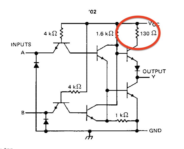
(excerpt from the datasheet)
I wanted to verify experimentally that the circuit really connects and disconnects from the bus, but I wasn’t sure what to expect with a multimeter. Measuring the output gave:
| State | Voltage |
|---|---|
Data = 1 |
3.3 V |
Data = 0 |
0 V |
| Disabled | 0 V |
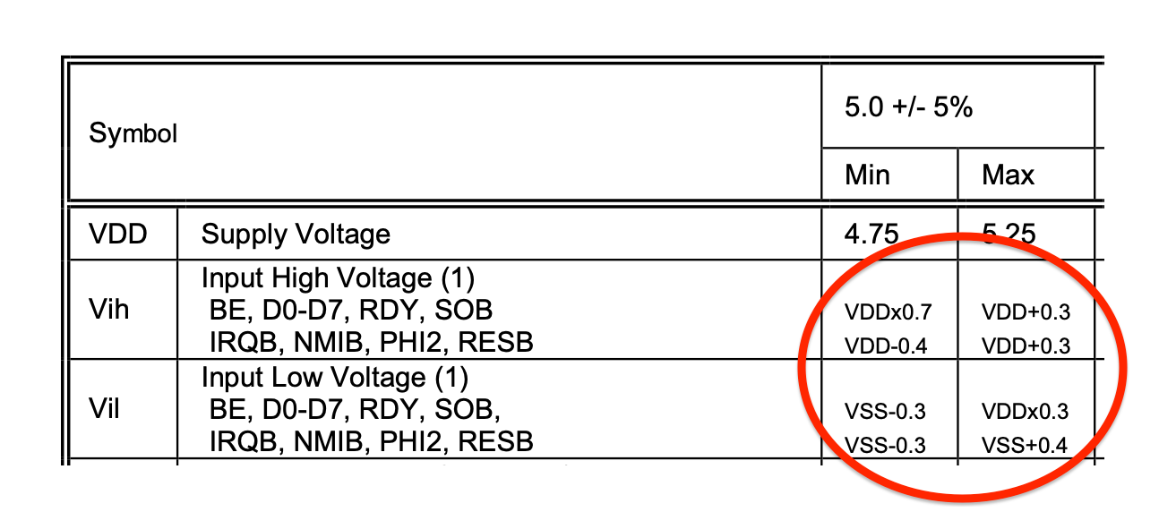
When outputting a 1, I measured 3.3 V. This is probably mostly due to the resistor located before the transistors. I hadn’t checked at the time, but the datasheet specifies guaranteed logic thresholds of 1.5 V for a 0 and 3.5 V for a 1. So we’re slightly below the guaranteed threshold for a logic high, but only by a small margin, and everything still worked correctly.
When the peripheral is supposed to be disconnected from the bus, I measured 0 V. However, the multimeter also displays 0 V when the probe is left floating, so I wasn’t sure I could conclude anything. When I asked ChatGPT how to verify that the output was truly in a high-impedance state, it suggested connecting a resistor between VDD or GND and the output. If the output is genuinely high impedance, the voltage should follow whichever rail it is connected to through the resistor. I tried it and confirmed that this was indeed the case. A more reliable test would have been to measure current, but I considered this sufficient.
Connecting to the 6502 and writing a test program
I rewired the transistors in a semi-permanent way to clean up the circuit and free a couple of wires. The idea now was to test the complete system with the 6502, the D latch, and the button. While doing so, I would also correct the latch design based on what I had learned about timing. The goal was to verify that the presence of the button on the bus did not interfere with the rest of the system.
Since the last session I had disconnected the latch for storage. Reconnecting it required digging out my schematics and chip pinout diagrams and matching everything back to the actual circuit. It took quite a bit of effort and concentration, especially because I was worried about making a mistake and damaging something. I made a mental note to think about better ways to manage this in the future.
I reconnected the latch and confirmed that it still worked just as before. Then I passed the clock signal through an inverter so that data would be captured on the falling edge instead of the rising edge. It seemed to work just fine—no noticeable difference from the previous test.
Finally I connected my button to data line D0. Since the program wasn’t yet reading the button, the output remained in a high-impedance state, and the LED simply reflected whatever data happened to be passing on the bus. Everything behaved as expected so far.
Now it was time for programming.
I reused the previous program and stripped it down to a loop that continuously reads the button state and writes it to the LED. As we saw earlier, the latch and button share the same address. A read activates the button; a write activates the latch.
The program is:
| Address (CPU) | Data | Instruction |
|---|---|---|
0x8000 |
AD 00 40 |
LDA $4000 |
0x8003 |
8D 00 40 |
STA $4000 |
0x8006 |
4C 00 80 |
JMP $8000 |
I reused the Arduino setup and code developed previously to erase the old program and write the new one in its place. After checking everything, I moved on to testing.
The first results left me puzzled. Then I suddenly realized that I had forgotten to power the CPU! I fixed that, but things were still not quite right. Then I noticed that I had forgotten to reinstall the ROM chip—it was still sitting in the programmer! My setups are still very experimental and require remembering a lot of details every time. Keeping everything in my head is not easy.
After fixing those issues, the results looked much better. I could clearly see the expected repetition caused by the loop, but the values were not quite correct. They were close, but different. Inspecting the data bus revealed that two wires had been swapped. Connecting an 8-wire ribbon cable to an already crowded breadboard is not easy, so this mistake didn’t surprise me at all.
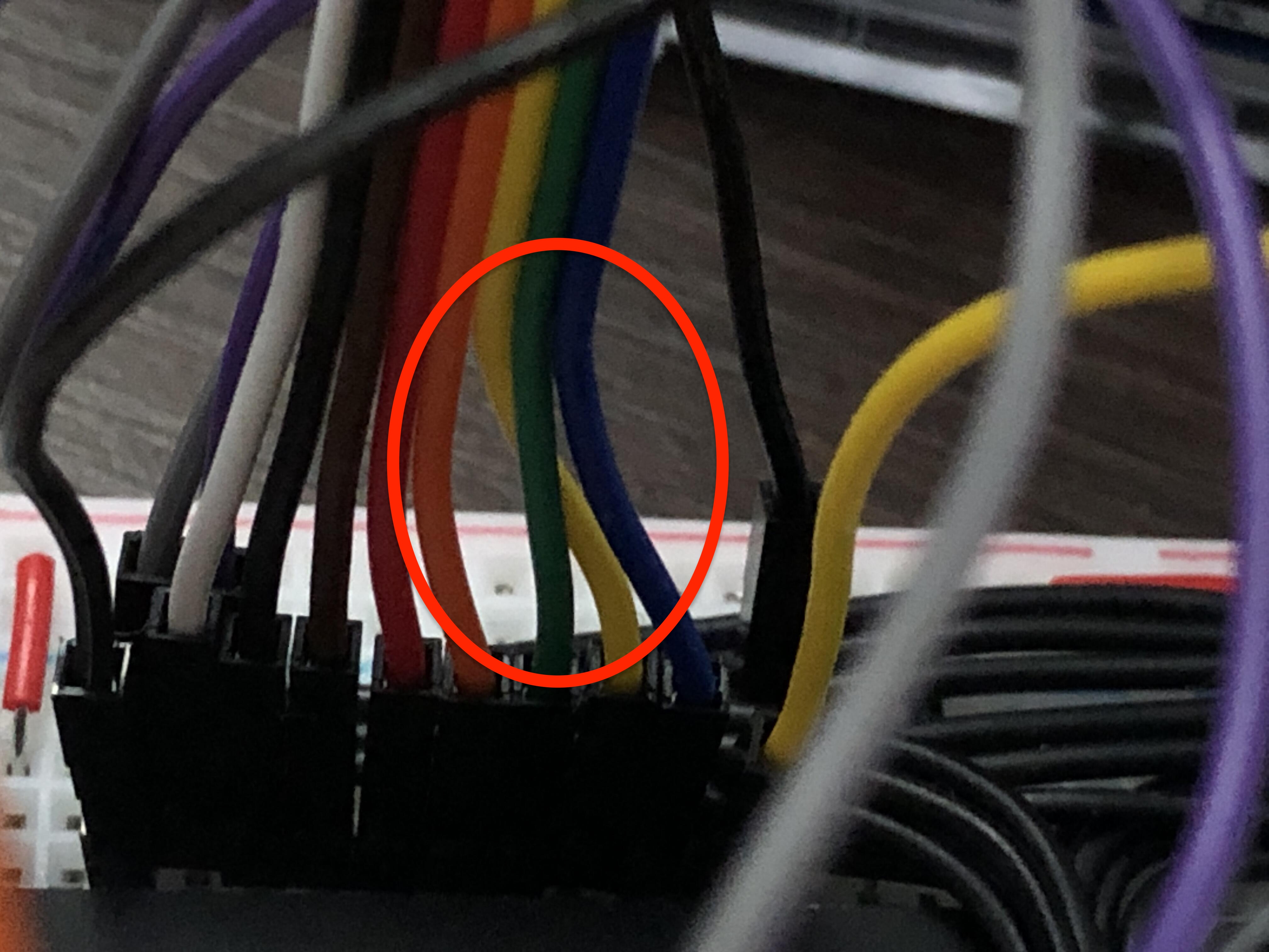
Overall everything worked well, but I identified two issues.
First, the value read by the CPU sometimes appeared as 0x40 or 0x41 instead of the expected 0x00 and 0x01. This is be because only D0 was connected to the button. The other data lines remained in a high-impedance state, leaving the CPU to read undefined values. In practice, those lines tended to retain the last value that had been present on the bus.
Second—and much more unexpectedly—I noticed that when the CPU wrote a 1 to the latch while it was already holding a 1, the output briefly switched to 0 for one clock cycle before returning to 1. That was very strange.
At first I had no idea what could be wrong. I spent quite a while watching the program execution and examining the values displayed by the Arduino, trying to understand the issue, but it remained mysterious.
Investigating latch issues
My first theory was that the latch was capturing data on the falling edge of the previous clock cycle. It was the only explanation that seemed plausible, although I couldn’t see how it could happen.
The 6502 timing diagram clearly indicates that the RW signal remains valid slightly beyond the falling edge of the clock. At the falling edge of the previous cycle it should still have the value “read”, which should prevent the latch from activating.
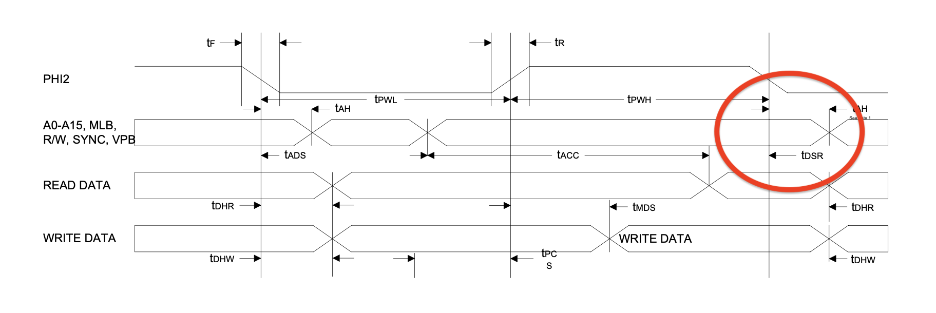
I then considered that the issue might come from the way I had implemented edge detection in the latch. I had connected all the signals (address, RW, clock) into the logic circuit first, and then fed the result into the edge detector. But with this architecture, it is entirely possible to generate a pulse outside of an actual clock edge. In fact, a pulse is generated whenever all the signals simultaneously reach their expected values.
The RW signal settles during the phase when the clock is low. Since I had inverted the clock signal going into the latch, the circuit sees a logical 1 at that moment and therefore generates a pulse as soon as RW becomes valid—which is definitely not what we want. I was quite proud of figuring this out.
I modified the circuit so that the edge detector was placed before the logic gates instead of after them. This way, latch activation would always be tied to an actual clock edge. I connected the signal that previously fed the edge detector directly to its destination, then rerouted the clock input through the detector and connected the detector’s output where the clock had originally gone.
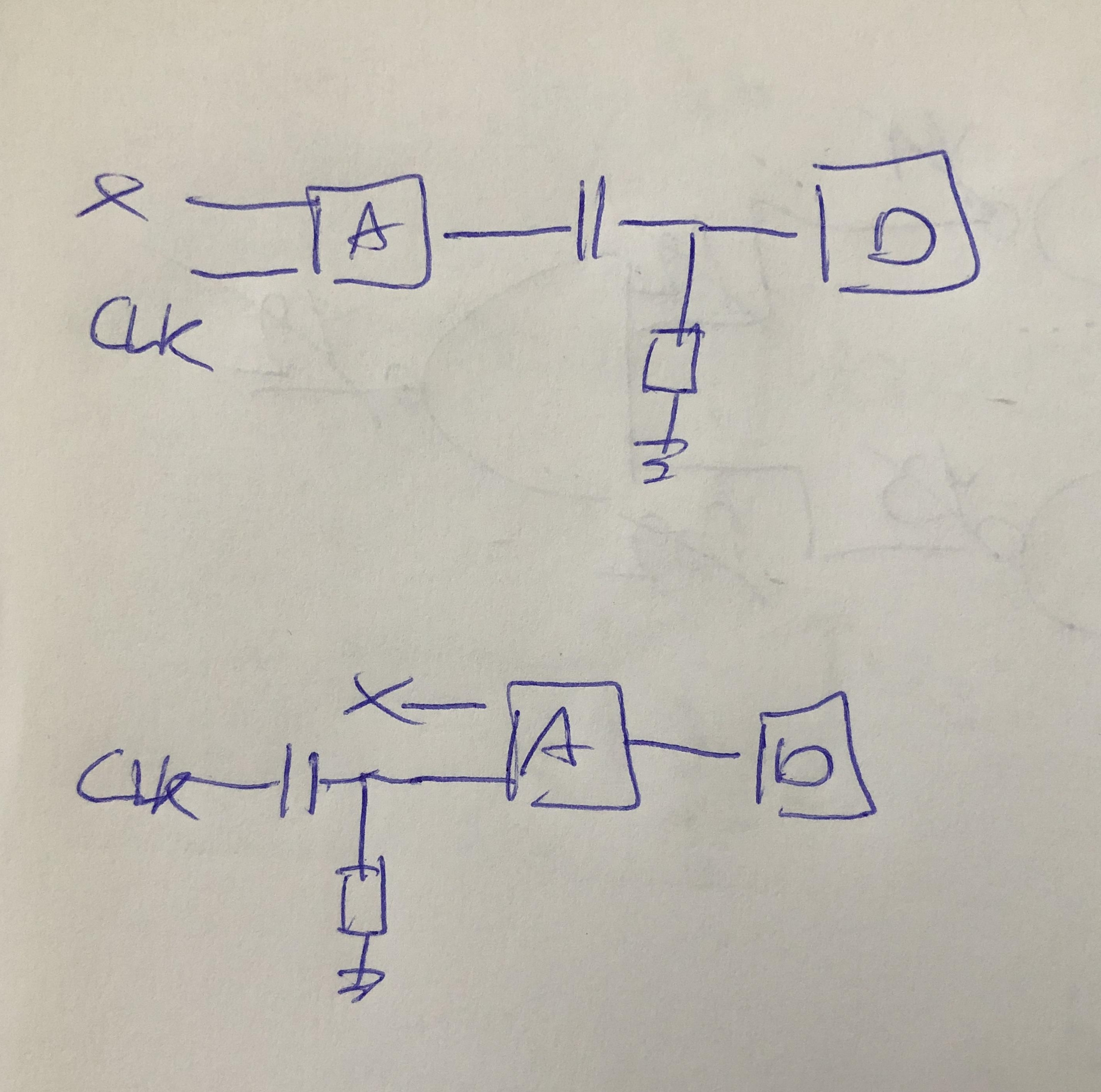
The RC circuit is used to detect signal edges.
At first it seemed to work because the LED no longer blinked off, but then I noticed that it remained permanently on—even when writing a 0. Perhaps I should have disconnected everything and verified my diagnosis before modifying the circuit directly. I had been very confident, but seeing the fix fail made me doubt my understanding.
I wondered whether this might be a timing issue or perhaps related to propagation delays through the logic gates. I forced the latch enable signal and observed that the latch copied the bus as expected (we say it is in a transparent state). I then connected the clock signal directly, without inversion and without the edge detector. That worked perfectly, although it didn’t feel conceptually correct. I wanted the latch to capture data on the falling edge of the clock. Given the timing analysis above, that seemed like the right way to do it.
I then considered that the pulse generated by my edge detector might be too short. Looking back, that didn’t really make sense. I still tried increasing the resistor value, going from roughly one hundred ohms to one megaohm, but it just reproduced the original problem. I then realized that, based on the 6502 timing diagrams, the pulse can’t really be “too short.” An arbitrarily short pulse should work in principle. However, propagation delays through the logic gates could indeed create issues.
The final circuit
I was feeling somewhat lost, so I asked ChatGPT for help, but at this point it was mostly to take some time to let my thoughts settle. I thought back to how RAM and ROM writes work, as explained in Ben Eater’s timing video. In reality, RAM or ROM continuously writes data whenever the chip is enabled and the write signal is active. It simply stops updating once one of those signals disappears. The trick is to enable the chip only during the period when the clock is high, because during that phase the 6502 guarantees that all control signals are valid and stable. If you don’t do this, signals may become invalid in an unpredictable order, potentially causing unintended writes.
The 6502 does not guarantee that write data remains valid throughout the entire high clock phase—only around the falling edge. Therefore, if memory becomes active as soon as the clock goes high, it may initially capture invalid data. However, because it continues capturing throughout the cycle, the final value captured is guaranteed to be valid. For RAM—or for my latch—that isn’t a problem. But I wondered whether there are situations where it would be.
Maybe there could be a second latch that would capture the output of the first one, this time latching on the actual falling edge of the clock. The first latch would continuously follow the bus during the write cycle, while the second would only capture the final stable value. Timing would no longer be an issue because the second capture occurs entirely between the two latches, and the first latch holds its value indefinitely. ChatGPT confirmed that this is indeed a common solution, and I was quite pround of my thinking.
The correct solution for my latch is therefore to leave it transparent while the clock is high. In practice, this means connecting the clock directly, with no inverter and no edge detector. I had already tested this configuration during my experiments, and it worked perfectly. I increased the clock speed to about 1 kHz, and the LED followed the button state with only a small delay.
Conclusion
In the end, this session was mostly an opportunity to explore timing and interoperability issues in depth. Before this, I only had a vague idea of what actually happens during a clock cycle. Now I have a much clearer understanding, and I’m very happy about that. I would not have learned all this if I had simply used the VIA chip as originally planned.
When I first installed the ROM, I remember wondering whether the CPU could somehow write to it. I concluded that it couldn’t, because the ROM expects the control signals to be orchestrated in a specific way that the CPU cannot do with only the address and data buses. I now understand that it would actually be possible. You simply need to include the clock signal in the Chip Select logic.
What’s next
Everything is now ready to start writing interactive programs, although the possibilities remain limited. I’m considering replacing the latch with registers such as the 74LS173 so that I can easily obtain as many outputs as I want. It would even be possible to build some kind of rudimentary display using an LED matrix. Similarly, for inputs, I could use chips such as the 74LS244 to connect multiple buttons easily. I also still need to add RAM (already ordered and currently awaiting delivery), which will allow programs to use the stack.
There is no need to wait until the system becomes very complex to start to explore emulation. In fact, it may even be better to begin with a very simple system. However, it is important that I find it enjoyable and fun, and at this point the most significant improvement toward that goal would be to make the overall setup cleaner and more permanent. In its current state it is not very practical, and the connections don’t inspire much confidence. Not to mention that it ties up a fair amount of hardware.
I’ve considered several approaches to make the setup cleaner. First, perfboards, but they don’t really appeal to me. I don’t find them particularly practical. Designing PCBs could be interesting—I recently had the opportunity to create my first PCB and really enjoyed it—but most manufacturers require ordering at least five or ten boards, which feels excessive for a design that is still evolving. The best solution might actually be homemade PCBs built on top of 3D-printed bases. I discovered this approach recently, and it could be a perfect use case. The copper sheets are already sitting in my AliExpress cart ;)
I use generative AI to write and/or translate the content featured on this website. AI serves only as a tool for productivity and inspiration, I make sure that the final texts always reflect my personal voice and style.