Entry #006 - Jun 7th, 2026
Introducing the 6522 "Versatile Interface Adapter"
I now have a 6502-based system that I can program. The goal now is to add LEDs and buttons so that I can write and run interactive programs.
The 6522’s role
The 6502 alone cannot directly drive LEDs or read buttons, because the only things it can do directly is read and write on the address and data buses. To drive an LED or read a button we need an intermediate system that interfaces with the LED or button on one side, and communicates with the CPU through the buses on the other side.
The 6522 is an interface chip designed to work with the 6502. Its full name is Versatile Interface Adapter, so I’ll simply refer to it as “the VIA”. The VIA provides several complementary functions, including timers, but our main interest here is its two parallel I/O ports. These are 16 lines that can each be configured individually as either inputs or outputs, and that we can read or write from the CPU.
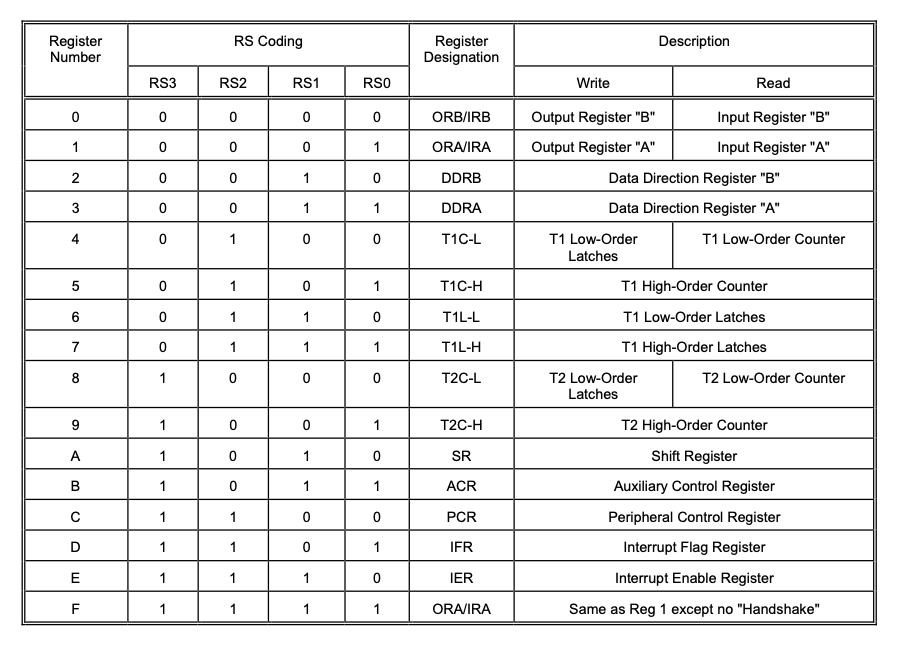
The VIA has 16 control registers that the CPU reads from or writes to through the data bus in order to perform the desired functions. The address bus is used to select which register to access. Since there are only 16 registers, 4 address lines are sufficient.
Chip Select and the address space
Up to now there was only one component connected to the address and data buses: the EEPROM. We are now adding the VIA, so we must ensure that the CPU can communicate with each component without disturbing the others or being disturbed by their presence on the bus. This is accomplished using the Chip Select (also known as Chip Enable) signal. The Chip Select signal allows the CPU to activate only the component it wants to communicate with at a given moment. Each component has one or more inputs for this signal and only takes control of the bus when the signal permits it. The rest of the time, the bus-connected pins are electrically disconnected from the bus, in what is known as an high-impedance state.
To determine which component should be active, we use the address bus. With 16 address lines, the CPU can generate 65,536 distinct addresses. These 65,536 addresses form what is known as the address space. The idea is to divide this address space into ranges and assign each range to a specific component. We do that by combining cleverly chosen address lines to produce the Chip Select signal for each component.
Until now I had tied the EEPROM’s Chip Select (/CE) low so that the ROM was always active. As a result, the entire address space was assigned to it. The ROM only has 15 address lines (32 KB addressable), and we left the 16th address line disconnected. Consequently, when the CPU uses an address in the range 0x0000–0x7FFF, it maps directly to an address in the ROM. But the same is true for addresses 0x8000–0xFFFF because looking at only the 15 first lines, the addresses are identical. From the CPU’s perspective, the ROM contents appear duplicated.
| Bin | Hex |
|---|---|
0000 0000 0000 0000 |
0x0000 |
0111 1111 1111 1111 |
0x7FFF |
1000 0000 0000 0000 |
0x8000 |
1111 1111 1111 1111 |
0xFFFF |
Since the 16th address line (A15) is not used to address data within the ROM, we can use it for Chip Select. If we connect it directly to the ROM’s /CE input, the chip —being active when the signal is 0— will only respond to addresses in the range 0x0000–0x7FFF. We have therefore allocated 0x0000–0x7FFF to the EEPROM and freed the remainder for other devices. However, recall that on startup the CPU reads addresses 0xFFFC and 0xFFFD (the reset vector), and with this memory layout that would no longer work. We could add a component whose sole purpose is to respond to those two addresses, but we would then have to keep its value updated according to where the program starts in ROM. A simpler solution is to allocate the range 0x8000–0xFFFF to the ROM instead. We can do this by inverting A15 (using a NOT gate) before connecting it to /CE. This way, address 0x7FFC in ROM corresponds to address 0xFFFC from the CPU’s perspective. On the other hand, ROM address 0x0000 becomes CPU address 0x8000. We’ll need to keep this in mind when writing programs later.
We can now consider how to allocate the address space to the VIA. We already know that its range must be within 0x0000–0x7FFF. We could allocate the entire range, and as long as we don’t add any other components this wouldn’t cause a problem. However, I plan to add at least one RAM chip later, so let’s do something a bit better.The VIA only has 16 registers, so in principle it only requires 16 addresses. Of course, its allocated range can be larger than that.
I’m starting to run out of breadboards, and the ones already in use are fairly crowded, so I’d like a solution that requires as few connections and components as possible. The VIA has two Chip Select signals: CS1 and /CS2. The chip is enabled when CS1 is 1 and /CS2 is 0. We already know that the VIA must be disabled whenever the 16th address line (A15) is 1, because that corresponds to the range assigned to the ROM. Therefore we can connect A15 directly to /CS2. If we stop there, we have effectively assigned the entire range 0x0000–0x7FFF to the VIA. Now imagine connecting A14 to CS1. The VIA would then only be active when A15 = 0 and A14 = 1, which corresponds to addresses 0x4000–0x7FFF. If we added A13 through an AND gate, we would reduce the range to 0x6000–0x7FFF. Adding A12 would further reduce it to 0x7000–0x7FFF. The more we shrink the allocated memory range, the more space we leave available for other devices, but the more logic is required to generate the Chip Select signals.
| Bin | Hex |
|---|---|
0000 0000 0000 0000 |
0x0000 |
0100 0000 0000 0000 |
0x4000 |
0110 0000 0000 0000 |
0x6000 |
0111 0000 0000 0000 |
0x7000 |
0111 1111 1111 1111 |
0x7FFF |
1000 0000 0000 0000 |
0x8000 |
1111 1111 1111 1111 |
0xFFFF |
For now, I choose to keep things simple and stop at A14. This allows CS1 and /CS2 to be connected directly without additional logic, and the address-space tradeoff is acceptable for the moment.
Summary of the required connections:
| Address line | Connection |
|---|---|
A15 |
ROM /CE through a NOT gate |
A15 |
VIA /CS2 |
A14 |
VIA CS1 |
Setting up the EEPROM with Chip Select and testing the program
I want to install the VIA and the Chip Select decoding logic semi-permanently on a large breadboard connected to the 6502 breadboard, but I’ve run out of large breadboards. I’ve ordered more, but while waiting for them to arrive I’m building a temporary setup on a small breadboard using Dupont jumper wires. This won’t leave enough jumpers to monitor the buses with the Arduino, but that’s fine.
To keep things simple, I use a 74LS04 chip which has 6 inverters on it, and I place it on the 6502 breadboard after the area reserved for the ROM. This is temporary, as I plan to put the RAM there later. I power the 74LS04, connect A15 to the input of the first inverter, remove the wire that had been tying the ROM’s /CE to ground, and connect the inverter output in its place.
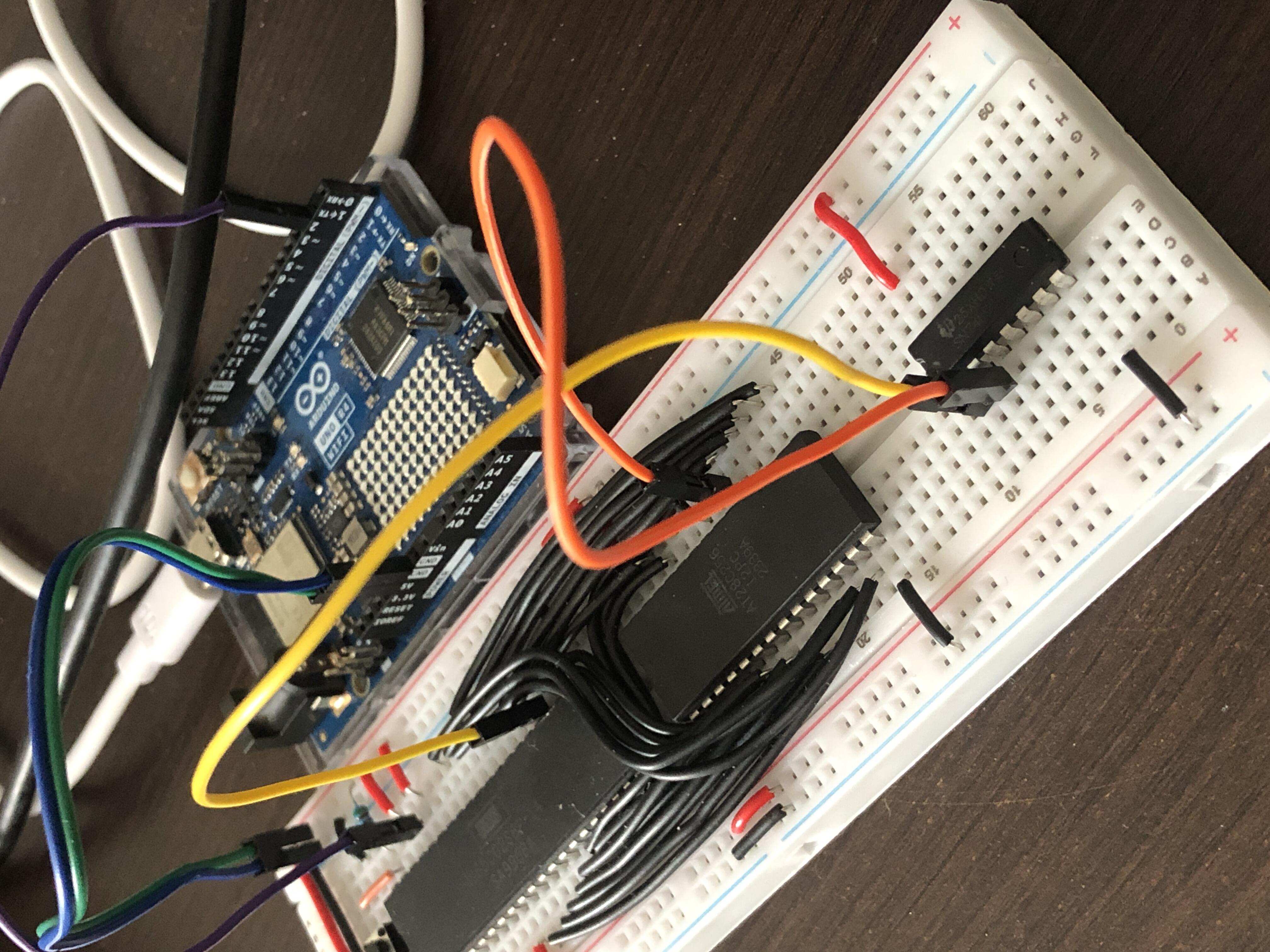
Before installing the VIA and committing the wiring, I need to reprogram the ROM. To avoid having to reprogram it again if things don’t work the first time —which currently requires rewiring the Arduino every time— I want a program whose effects are unmistakable. I imagine a program that blinks three LEDs with an alternating pattern of 010-101. There’s no need for a counter or timer; with a sufficiently slow clock the pattern will visibly blink even if the instructions execute back-to-back without any delay.
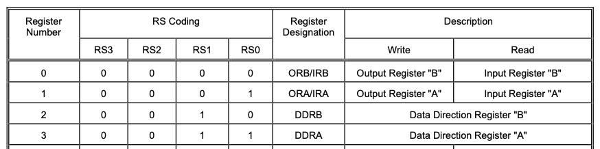
At this point it’s worth taking a closer look at how the VIA works. To configure the Port A pins as outputs, we need to write to register 3. Any bit set to 1 in that register configures the corresponding pin as an output. Then, to set the output value on the pins, we write to register 1. Given the memory mapping we established earlier, the addresses for registers 1 and 3 are 0x4001 and 0x4003, respectively.
So our program essentially looks like this:
- Write
1111 1111(0xFF) to address0x4003 - Write
0000 0010(0x02) to address0x4001 - Write
0000 0101(0x05) to address0x4001 - Repeat from step 2
In pseudo machine code, this becomes:
LDA #$FFSTA $4003LDA #$02STA $4001LDA #$05STA $4001JMP $XXXX
Explanation: To write a value into a VIA register, we first load the value into the accumulator, then store the accumulator’s value at the register’s address. The JMP instruction moves the execution pointer to the specified address. Here we want to jump back to LDA #$02 to form an infinite loop. To determine the correct address for the JMP, we need to know:
- where the program starts in memory,
- how many bytes the preceding instructions occupy,
- and how the address space is mapped.
For simplicity, we can place the program at ROM address 0x0000, which corresponds to CPU address 0x8000. We’ll therefore need to place that value in the reset vector.
We have already encountered the STA instruction before. Its opcode is 0x8D, and the target address is supplied in the next two bytes, least significant byte first. We have also encountered LDA, but previously we used the version that loads from a memory address. Here we want to give it a value directly, this is called the immediate addressing mode. The datasheet tells us that the opcode for this version of LDA is 0xA9, followed by the value byte. Now let’s look at JMP. It also exists in several addressing modes. Here we want the absolute-address mode, whose opcode is 0x4C, followed by the two-byte address (least significant byte first, as always).
Here is the final program:
| CPU Address | ROM Address | Data |
|---|---|---|
0x8000 |
0x0000 |
A9 FF |
0x8002 |
0x0002 |
8D 03 40 |
0x8005 |
0x0005 |
A9 02 |
0x8007 |
0x0007 |
8D 01 40 |
0x800A |
0x000A |
A9 05 |
0x800C |
0x000C |
8D 01 40 |
0x800F |
0x000F |
4C 05 80 |
0xFFFC |
0x7FFC |
00 |
0xFFFD |
0x7FFD |
80 |
We can see that the LDA #$02 instruction ends up at address 0x8005, so that is the address we give to JMP. I program the ROM using the setup defined earlier and reinstall it in the circuit.
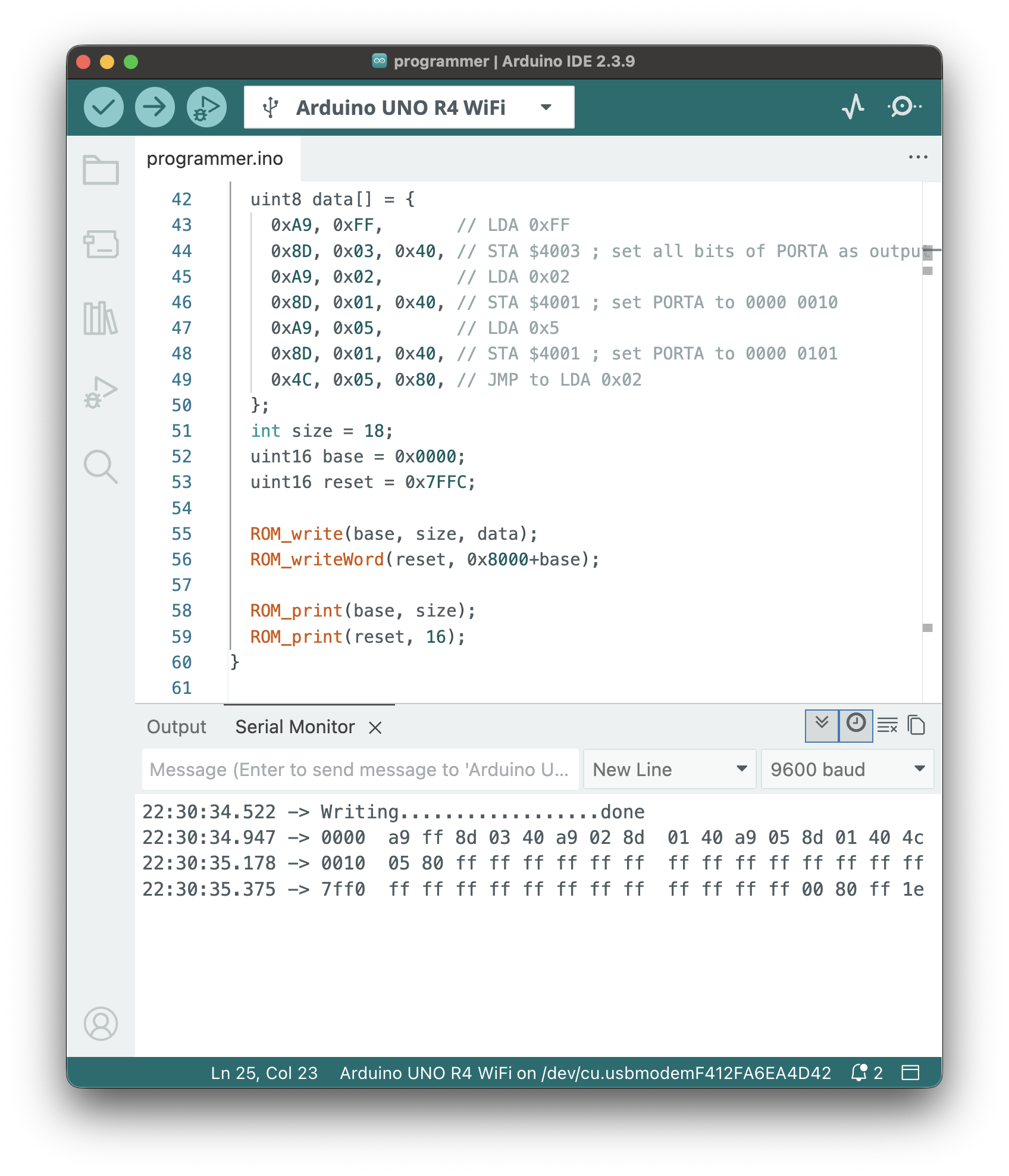
Before installing the VIA, I verify that the Chip Select logic works correctly and that the program is valid. I connect the Arduino to the bus and observe the signals, still monitoring only the first four address lines. Here is what I captured:
| Address (theory) | Addresse (observed) | R/W | Data |
|---|---|---|---|
0xFFFc |
0xc |
R |
0x00 |
0xFFFd |
0xd |
R |
0x80 |
0x8000 |
0x0 |
R |
0xa9 |
0x8001 |
0x1 |
R |
0xff |
0x8002 |
0x2 |
R |
0x8d |
0x8003 |
0x3 |
R |
0x03 |
0x8004 |
0x4 |
R |
0x40 |
0x4003 |
0x3 |
W |
0xff |
0x8005 |
0x5 |
R |
0xa9 |
0x8006 |
0x6 |
R |
0x02 |
0x8007 |
0x7 |
R |
0x8d |
0x8008 |
0x8 |
R |
0x01 |
0x8009 |
0x9 |
R |
0x40 |
0x4001 |
0x1 |
W |
0x02 |
0x800a |
0xa |
R |
0xa9 |
0x800b |
0xb |
R |
0x05 |
0x800c |
0xc |
R |
0x8d |
0x800d |
0xd |
R |
0x01 |
0x800e |
0xe |
R |
0x40 |
0x4001 |
0x1 |
W |
0x05 |
0x800f |
0xf |
R |
0x4c |
0x8010 |
0x0 |
R |
0x05 |
0x8011 |
0x1 |
R |
0x80 |
0x8005 |
0x5 |
R |
0xa9 |
0x8006 |
0x6 |
R |
0x02 |
0x8007 |
0x7 |
R |
0x8d |
0x8008 |
0x8 |
R |
0x01 |
0x8009 |
0x9 |
R |
0x40 |
0x4001 |
0x1 |
W |
0x02 |
0x800a |
0xa |
R |
0xa9 |
0x800b |
0xb |
R |
0x05 |
0x800c |
0xc |
R |
0x8d |
0x800d |
0xd |
R |
0x01 |
0x800e |
0xe |
R |
0x40 |
0x4001 |
0x1 |
W |
0x05 |
0x800f |
0xf |
R |
0x4c |
0x8010 |
0x0 |
R |
0x05 |
0x8011 |
0x1 |
R |
0x80 |
The results are exactly as expected.
Installing the VIA
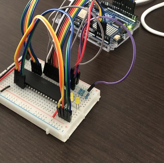
Finally here we are. I place the 6522 on a small breadboard and immediately connect VDD and VSS. I add three LEDs with their resistors and connect them to the first three outputs of Port A. I then go through the remaining pins. We need to connect:
- the 8 data lines (
D0toD7) - the 4 address lines (
A0toA3) - the read/write signal (
/RW) - the clock (
PHI2) - the reset signal (
/RES) CS1and/CS2
Until now we did not used the read/write signal (/RW) because the ROM is read-only, we only read from it. The VIA, however, supports both reading and writing, even though our test program only performs writes for now. The clock and reset signals can be connected directly to the corresponding signals on the 6502. I wire everything up, with the Arduino continuing to provide the clock signal as usual.
I start the system, perform a reset, and nothing happens. The LEDs remain off. This leaves me puzzled. I first check the LEDs by directly connecting them to 5V, and they light up correctly. Next I monitor the VIA outputs with the Arduino, and they all remain at zero. I also verify the CS1, /CS2, clock, and /RW signals, and everything appears correct. /RW stays high most of the time to indicate reads, and occasionally goes low for exactly one cycle during writes. Similar things for CS1 and /CS2.
I decide to try driving the VIA directly from the Arduino, both to verify that I can make it work manually and to confirm that the test program is indeed sending the correct commands. On the breadboard I force CS1 high, /CS2 low, and /RW low. In the Arduino code I perform a reset by pulling /RES low and generating a few clock cycles, then send the bytes needed to configure Port A. Still nothing. I try Port B instead. Still nothing. At this point I begin to suspect that the VIA I got may be defective.
I then attempt to read inputs from the ports. I modify the code to support both reading and writing through /RW that I connect to the Arduino, and connect 5V directly to one of the input pins. That’s when I realize the LEDs are still connected to Port A while I’ve moved to Port B. I fix that and repeat the previous tests, but still nothing. I perform the input read test and get 0. At this point I’m genuinely perplexed.
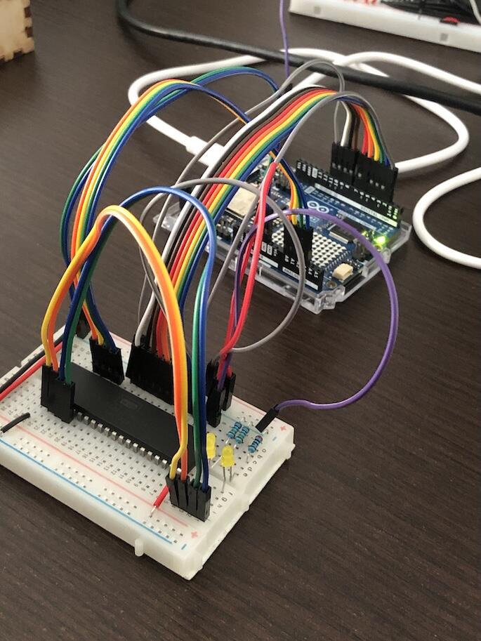
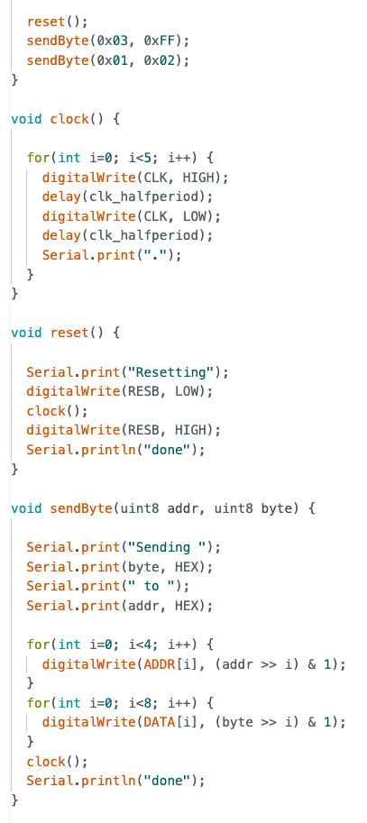
Arduino code is available on GitHub.
What’s Next
I haven’t managed to get the 6522 working, but after rewatching Ben Eater’s video where he uses it, I got the idea of building a latch like the one he demonstrated in this video and trying to interface it with the CPU. It’s an interesting exercise. If it works, it will provide a first CPU-controlled output device, which means I can finally observe results directly and start writing programs that actually do something.
I use generative AI to write and/or translate the content featured on this website. AI serves only as a tool for productivity and inspiration, I make sure that the final texts always reflect my personal voice and style.