Entry #003 - Jun 4th, 2026
EEPROM setup and connection to the 6502
The EEPROM is written and I have confirmed that it is working with the 6502 as expected. The goal today is to connect the ROM in a semi-permanent way to the 6502 on the same breadboard and wire all the address and data lines correctly. But before that I need to revise the ROM programming, because this time the address lines will be correctly wired and the CPU will therefore not find the data I previously programmed using the wrong address lines. There is also the fact that at startup, the CPU reads the reset vector at addresses 0xFFFC and 0xFFFD to know where it should start executing instructions from. With 4 address lines it was possible to place the reset vector at addresses 0x000C and 0x000D, but this will no longer work with full addressing.
The ROM uses 15 address lines (32KB addressable), while the CPU uses 16 (64KB addressable). For now I connect the first 15 lines and leave the CPU’s 16th line unconnected. Thus, when the CPU requests address 0xFFFC, it will correspond to address 0x7FFC in the ROM. That is therefore where the reset vector must go. We can then place the program anywhere in memory, as long as we specify the corresponding address in the reset vector.
I decide to start by writing the program at address 0x0000, write the reset vector later. I go back to my programming setup and connect all address lines to 0, while making sure to leave the actual 4 least significant address lines adjustable. I run the programming using the same Arduino code as before.
To write the reset vector, I decide for simplicity to write the entire program again at address 0x7FF0, which allows me to repear the same operation but with the address lines set to 1. The reset vector being 00 00, it should work, however to make things more interesting I decide to modify the value and set it to 0xFFF0, which will cause the program located at 0x7FF0 to execute instead of the one at 0x0000.
Summary of the writes to the ROM:
| Addr | Data | Comment |
|---|---|---|
0x0000 |
AD 09 00 |
LDA $0009 |
0x0003 |
AD 0A 00 |
LDA $000A |
0x0006 |
6D 0B 00 |
ADC $000B |
0x0009 |
28 |
|
0x000A |
02 |
|
0x000B |
0A |
|
0x000C |
00 |
|
0x000D |
00 |
|
0x7FF0 |
AD 09 00 |
LDA $0009 |
0x7FF3 |
AD 0A 00 |
LDA $000A |
0x7FF6 |
6D 0B 00 |
ADC $000B |
0x7FF9 |
28 |
|
0x7FFA |
02 |
|
0x7FFB |
0A |
|
0x7FFC |
F0 |
|
0x7FFD |
FF |
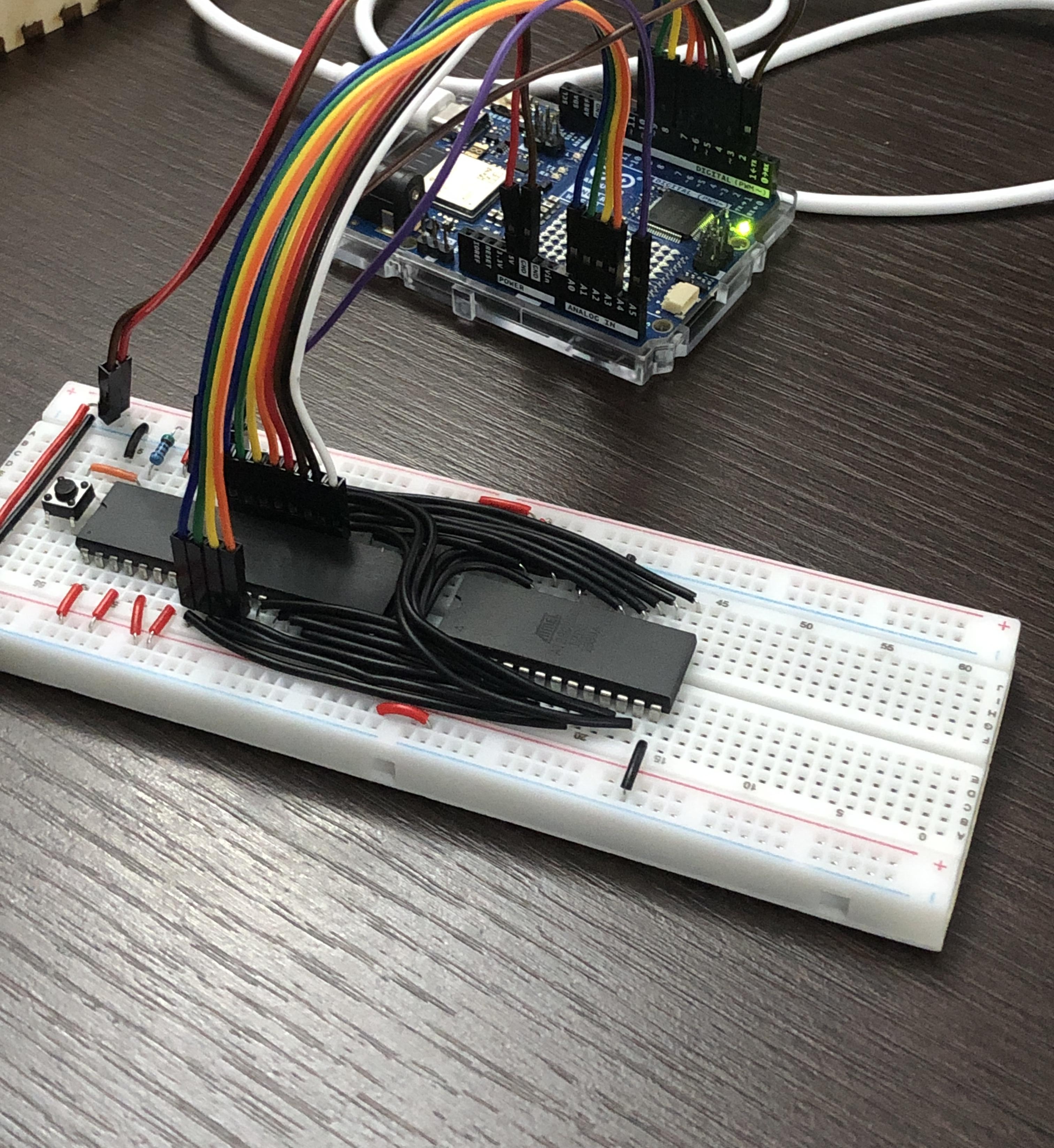
The ROM now ready, I install it on the breadboard next to the 6502. I force /CE to 0, /OE to 0, and /WE to 1, making the ROM always active and in read mode. I then connect the address lines and data lines. I try to do something nice, inspired by Ben Eater’s techniques.
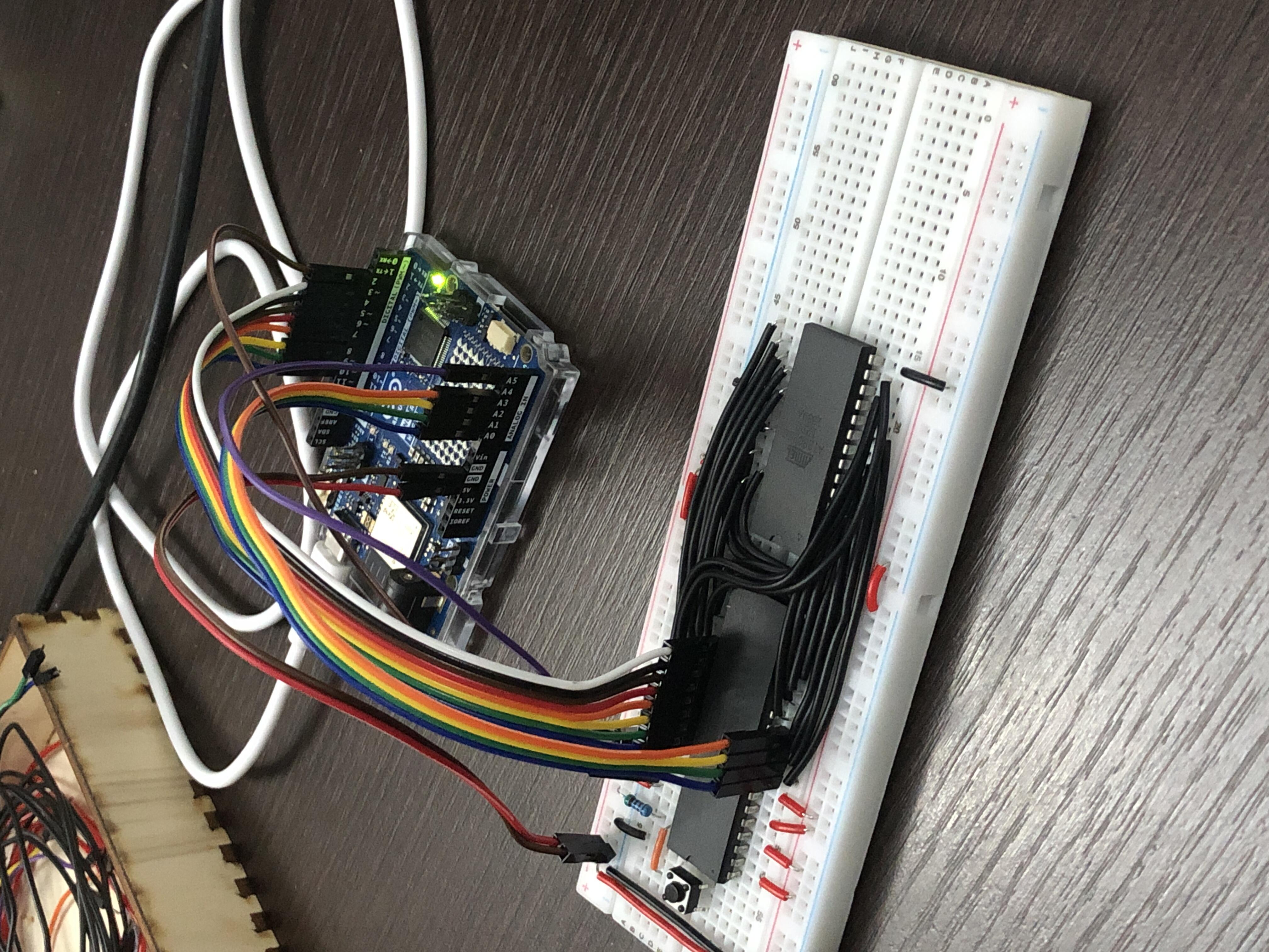
For observation I use ribbon cables for the buses; it’s cleaner than loose jumper wires. As before, the Arduino provides the clock, and I only observe the 4 least significant bits of the address.
I power up the board, reset the CPU, and here is the result:
| Address (theory) | Address (observed) | Data |
|---|---|---|
0xFFFC |
0xC |
f0 |
0xFFFD |
0xD |
ff |
0x7FF0 |
0x0 |
ad |
0x7FF1 |
0x1 |
09 |
0x7FF2 |
0x2 |
00 |
0x0009 |
0x9 |
28 |
0x7FF3 |
0x3 |
ad |
0x7FF4 |
0x4 |
0a |
0x7FF5 |
0x5 |
00 |
0x000a |
0xA |
02 |
0x7FF6 |
0x6 |
6d |
0x7FF7 |
0x7 |
0b |
0x7FF8 |
0x8 |
00 |
0x000b |
0xB |
0a |
Everything works as expected 🎉
Next
The system is now capable of reading arbitrary long programs, which is nice, but we still need to be able to program more than 16 bytes at a time. I have a few ideas for that. The next goal will be to use an input/output chip that will allow peripherals to be connected and finally produce observable results.
I use generative AI to write and/or translate the content featured on this website. AI serves only as a tool for productivity and inspiration, I make sure that the final texts always reflect my personal voice and style.