Entry #002 - Jun 2nd, 2026
Running our first program and introducing the EEPROM
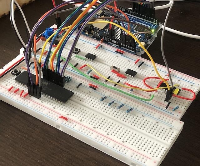
The 6502 is setup on a breadboard and I have confirmed that it is working as expected. For now the data 0xEA is hard wired on the data bus. The goat today is to provide the CPU with dynamic data based on the address it requests, so that it can execute a meaningful program. Traditionally, this is the role of a memory chip. For now, however, I am experimenting with Arduino.
Dynamic data
In addition to the 4 address lines used so far, I add the 8 data bus lines. I also connect the read/write signal to detect when the CPU is attempting to read from the bus.
Before going any further, I rework the program to display the new data, and I also make the Arduino generate the clock signal. This makes it easier to coordinate bus operations with the clock and allows me to freely adjust the clock speed. The 555-based module I was using, although adjustable, cannot go as low as I want.
I now write code that places 0xEA on the bus whenever the CPU is performing a read operation.
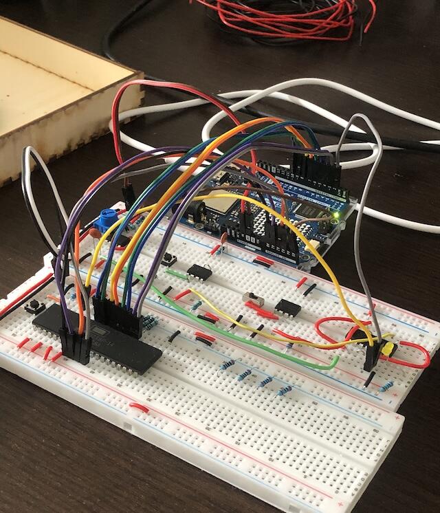
Now that we can provide dynamic data to the CPU, we can try to make it execute a small program. Very small, in fact, because since I am only working with 4 address bits, I can provide only 16 bytes in total, including the two bytes of the reset vector located at addresses 0xC and 0xD. Technically, I could have added one or two extra wires, which would have doubled or quadrupled the available space, respectively, but I thought it would be nice challenge.
To make things interesting, I choose instructions that generate both memory reads and writes. The LDA (Load Accumulator) instruction loads into the accumulator the value stored at the specified address. ADC (Add with Carry) adds to the accumulator the value read from the specified address. STA (Store Accumulator) writes the contents of the accumulator back to memory. Each of these instructions takes a two-byte memory address as a parameter, with the low byte first. With just three instructions we are already at 9 bytes. Immediately after I place the two data bytes that will be added by the CPU. That leaves only a single free byte before the reset vector.
Here is the final program (data shown in hexadecimal):
| Addr | Instruction | Data |
|---|---|---|
0x0 |
LDA $0009 |
AD 09 00 |
0x3 |
ADC $000A |
6D 0A 00 |
0x6 |
STA $000B |
8D 0B 00 |
0x9 |
28 |
|
0xA |
02 |
|
0xB |
||
0xC |
00 |
|
0xD |
00 |
|
0xE |
||
0xF |
Explanation:
LDA$0009: Load the value at address0x09into the accumulator.ADC$000A: Add the value at address0x0Ato the value currently in the accumulator.STA$000B: Store the value currently in the accumulator at address0x0B.
We should therefore observe the following events on the bus:
| Addr | R/W | Data | Event |
|---|---|---|---|
| 0xC | R | 00 | Reading the reset vector |
| 0xD | R | 00 | |
| 0x0 | R | AD | Reading the first instruction |
| 0x1 | R | 09 | |
| 0x2 | R | 00 | |
| 0x9 | R | 28 | Reading the data |
| 0x3 | R | 6D | Reading the second instruction |
| 0x4 | R | 0A | |
| 0x5 | R | 00 | |
| 0xA | R | 02 | Reading the data |
| 0x6 | R | 8D | Reading the third instruction |
| 0x7 | R | 0B | |
| 0x8 | R | 00 | |
| 0xB | W | 2A | Writing the data |
The result matches exactly what was expected:
Arduino code is available on GitHub.
Using an EEPROM
The Arduino is nice and all, but in the final system the data will be stored in a memory chip. Here I am using a 32KB AT28C256 EEPROM. This type of memory is intended to be used as read-only memory, but it can be erased and programmed electronically.
I want to start with the basics by performing reads and writes by manipulating the control signals manually. On a breadboard I connect eight LEDs to the ROM’s data bus and force all address lines to zero using jumpers, except for the four least significant bits, which I connect with easily repositionable jumper wires.
The ROM chip has three control signals:
| Signal | Meaning | Purpose |
|---|---|---|
/CE |
Chip Enable | Activates the chip |
/OE |
Output Enable | Drives the data bus |
/WE |
Write Enable | Triggers a write operation |
On the breadboard, I tie /CE to 0 to enable the chip and manually control /OE and /WE.
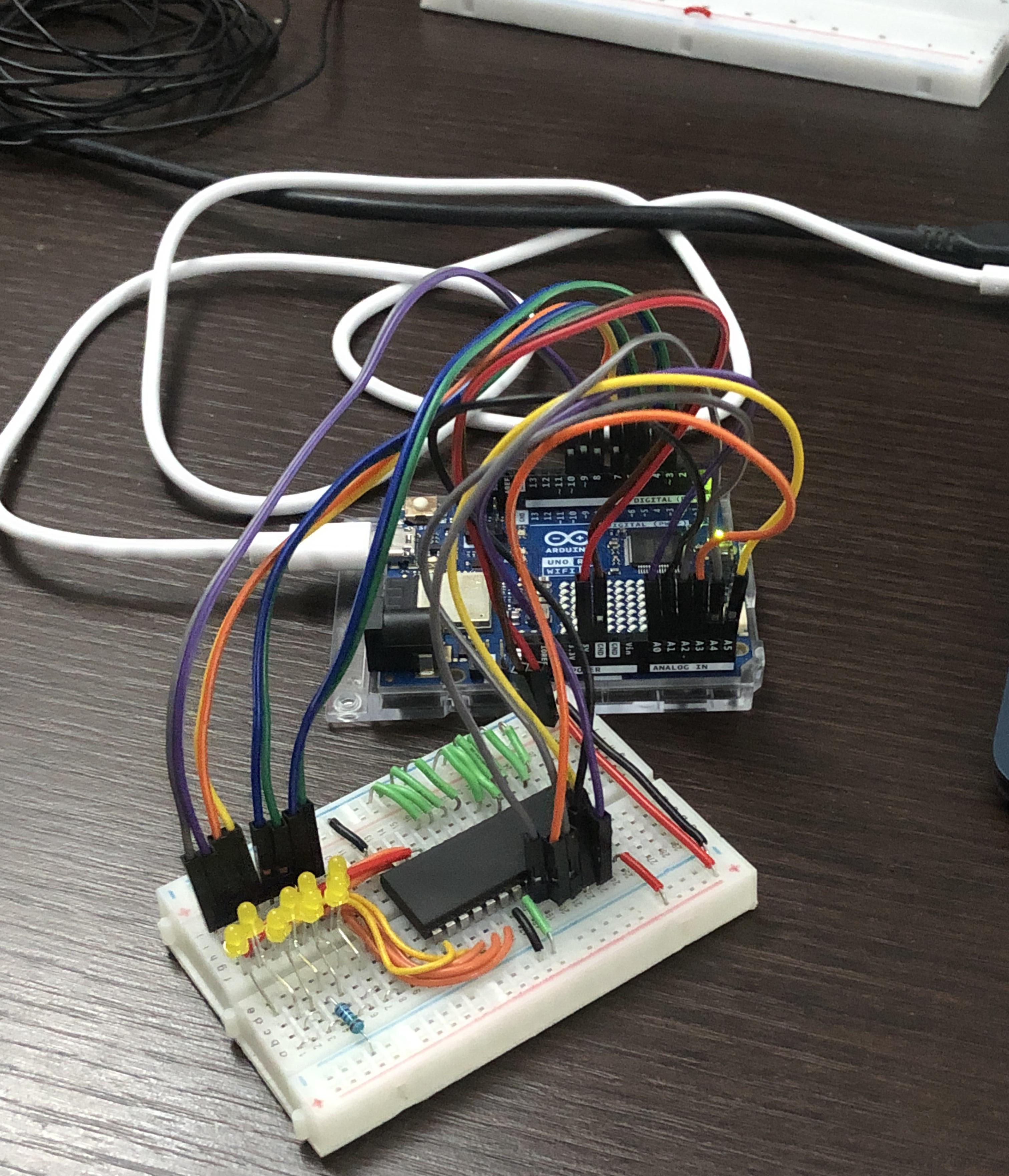
I start by testing reads. I set /OE to 0 to enable the outputs and /WE to 1 to place the chip in read mode, then cycle through the addresses by repositioning the four dedicated wires. The LEDs display the value stored at each address.
Here are the results:
| Address | Data |
|---|---|
0x0000 |
00 |
0x0001 |
FF |
0x0002 |
00 |
0x0003 |
FF |
0x0004 |
00 |
0x0005 |
FF |
0x0006 |
00 |
0x0007 |
FF |
0x0008 |
FF |
0x0009 |
FF |
0x000A |
FF |
0x000B |
FF |
0x000C |
FF |
0x000D |
FF |
0x000E |
FF |
0x000F |
FF |
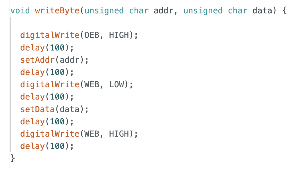
Next, I test writing. The process works as follows: under normal conditions (read mode), /WE is high. When /WE goes low, the chip captures the address present on the address bus. When /WE returns high, it captures the data and writes it to memory.
I first disable the outputs by setting /OE high. I configure address 0, then place the value 0xEA on the data bus using jumpers and verify it on the LEDs. Finally, I toggle /WE low and then high again.
I switch back to read mode by removing the jumpers from the data lines and setting /OE low. 0xEA appears on the LEDs. I check the other addresses and find the same values as before, except at address 0 that now contains 0xEA. First manual write successful!
I then connect the address lines, data lines, and control signals to the Arduino and write a program to automate reads and writes.
Initially, the program sequentially scans the 16 addresses and displays the corresponding data. It works well, and I retrieve the original values with OxEA at address 0. I then implement writing, starting with a function that writes a single byte. It reproduces the same control signal sequence that I had previously performed manually. After that, I add support for writing a sequence of values one byte at a time.
Arduino code is available on GitHub.
Connecting the EEPROM to the 6502
The goal now is to connect the ROM to the CPU so that it can read and execute the program. Leaving the ROM on its breadboard, I connect the four address lines and the data bus to the corresponding pins on the 6502. While doing this, I realize that the address lines I choose to manipulate on the ROM were not actually the four least significant bits as I intended. They were in fact lines 13, 8, 9, and 11. That is actually not an issue. As long as I connect the same line to the CPU in the same way, it will find the data at the expected address.
To analyze the results, I decide to rely on the LEDs connected to the ROM’s data bus. This is not necessarily the most convenient method, and I could connect the Arduino as before, but I do not want to add even more jumper wires to an already crowded setup. More importantly, I like to take every opportunity to compare my predictions against reality. Sometimes it highlights gaps in my understanding.
Before running the test, I modify the program so that the bus remains in read mode. I remove the STA instruction and slightly reorganize the program. Here is the new version:
| Addr | Instruction | Data |
|---|---|---|
0x0 |
LDA $0009 |
AD 09 00 |
0x3 |
LDA $000A |
AD 0A 00 |
0x6 |
ADC $000B |
6D 0B 00 |
0x9 |
28 |
|
0xA |
02 |
|
0xB |
0A |
|
0xC |
00 |
|
0xD |
00 |
|
0xE |
||
0xF |
If everything works correctly, we should observe the following data on the bus:
| Hex | Binary | Explanation |
|---|---|---|
| 00 | 0000 0000 | Reset vector |
| 00 | 0000 0000 | |
| AD | 1010 1101 | First instruction |
| 09 | 0000 1001 | |
| 00 | 0000 0000 | |
| 28 | 0010 1000 | Data |
| AD | 1010 1101 | Second instruction |
| 0A | 0000 1010 | |
| 00 | 0000 0000 | |
| 02 | 0000 0010 | Data |
| 6D | 0110 1101 | Third instruction |
| 0B | 0000 1011 | |
| 00 | 0000 0000 | |
| 0A | 0000 1010 | Data |
My first observations left me puzzled. The results did not seem to match my expectations, and I started wondering what was wrong. The 02 byte (0000 0010) made me suspect that the data was showing backwards, but that did not make much sense to me, until I realized that I was reading the LEDs backwards. I expected to see the same bit pattern as the numbers displayed on my screen, but the LEDs had the least significant bits on the left rather than on the right. I turned the board around and it seemed to match pretty well. I recorded the sequence to analyze it afterward, and confirmed everything matches perfectly.
What’s Next
The next goal is to connect the ROM to the 6502 in a more permanent way on the same breadboard, wiring up all address and data lines as well as the chip-enable logic. To do that, it will be useful to be able to program the entire memory space, and I have a few ideas about how to achieve this. After that, I can start installing the I/O chip that will make it possible to produce more directly observable results, and maybe drive some peripherals?
I use generative AI to write and/or translate the content featured on this website. AI serves only as a tool for productivity and inspiration, I make sure that the final texts always reflect my personal voice and style.