Jun 15th, 2026
Assembling the PCB for my media remote controller
Introduction
When I watch movies at home, I’m constantly adjusting the volume, skipping backward or forward, enabling or disabling subtitles, pausing and resuming playback, and so on. I use my Mac to watch movies on a large screen from my couch, which means I need to keep a wireless keyboard on my lap to control playback.
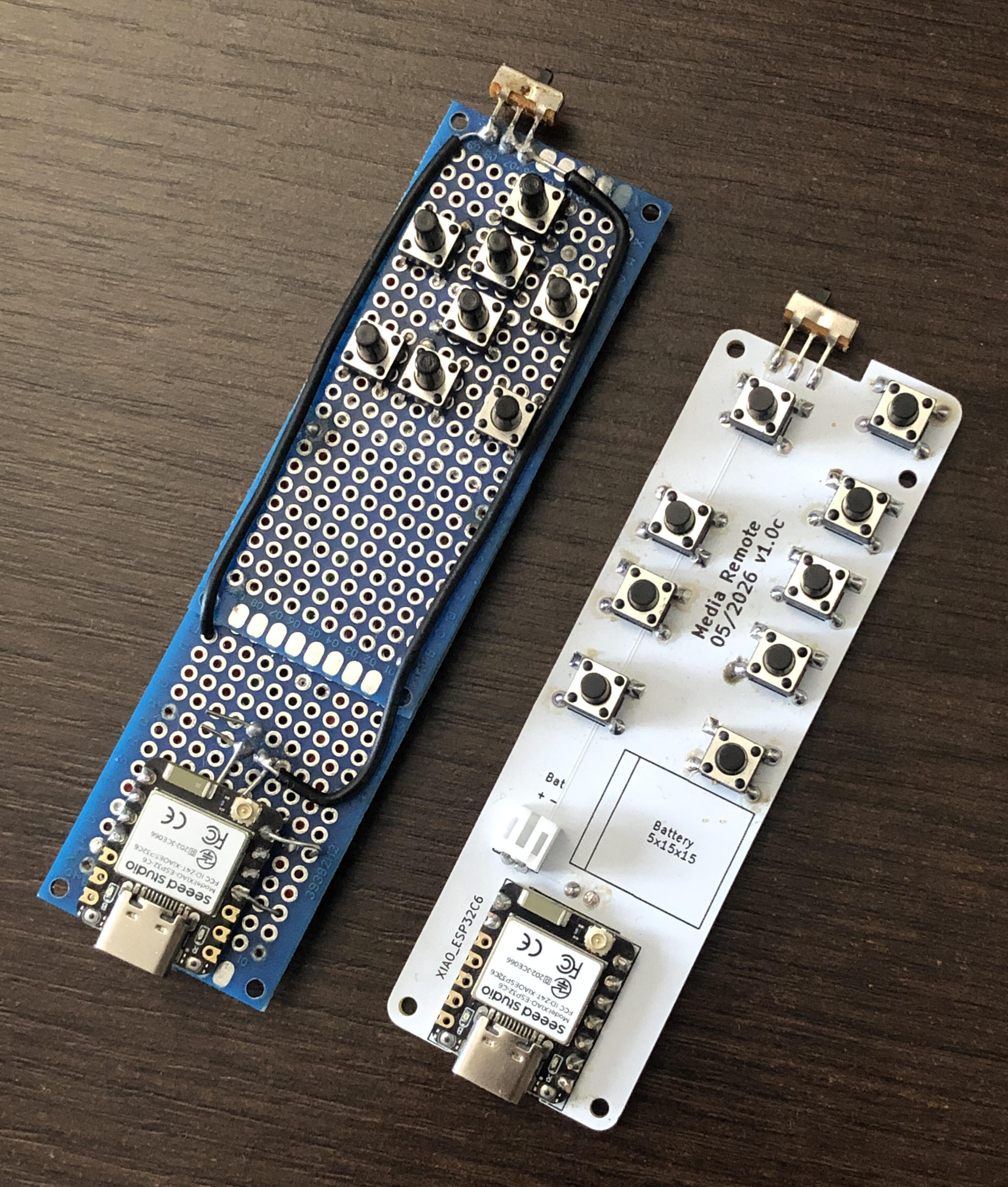
For some time now, I’ve been working on a remote control project that would be less cumbersome than a full keyboard. The system is based on an ESP32-C6 programmed to present itself to the computer as a Bluetooth keyboard. Buttons trigger the transmission of specific key presses, and a small battery powers the device. I recently completed a first prototype built on perfboard with a 3D-printed enclosure, and I’m very happy with the result.
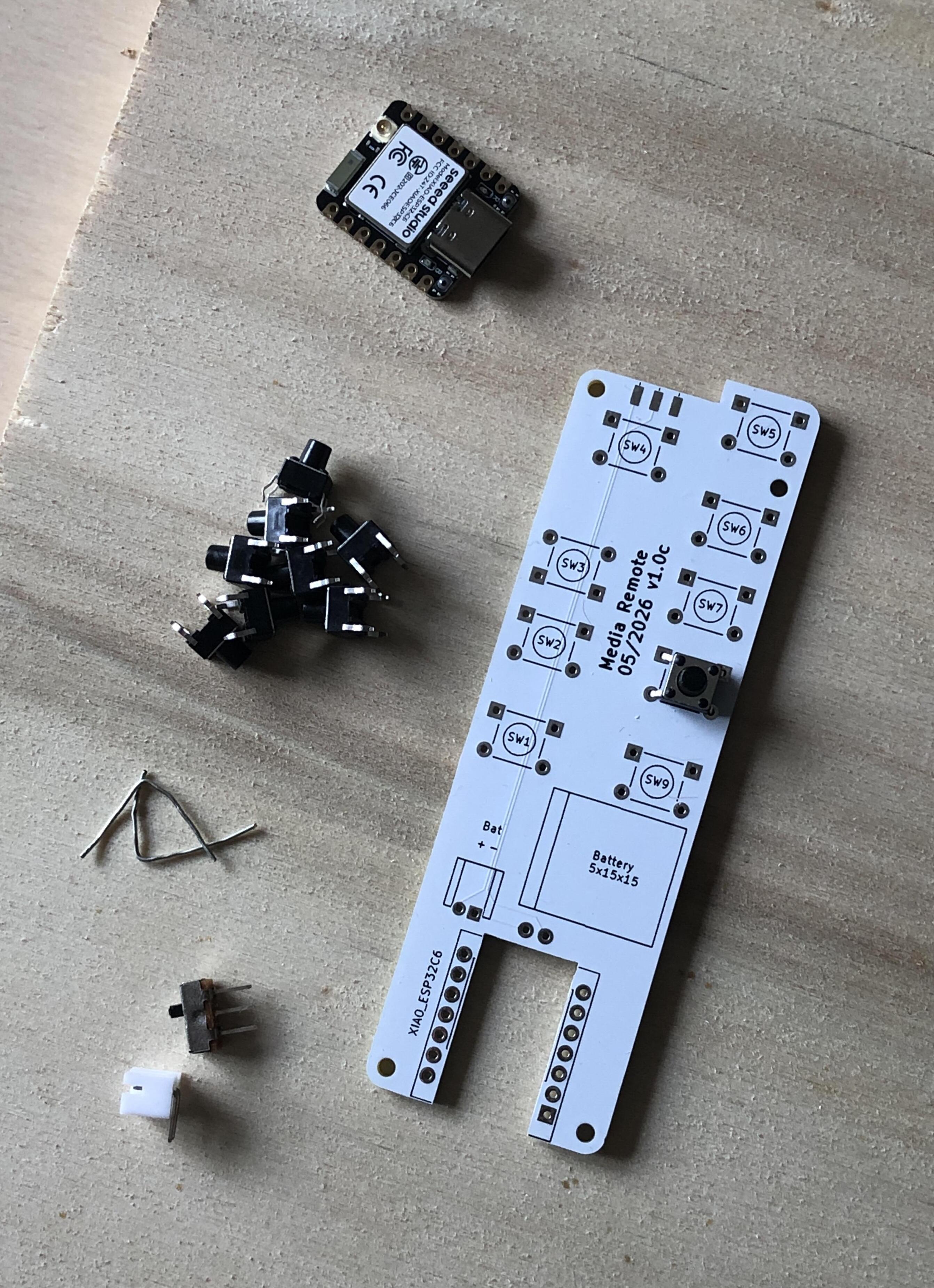
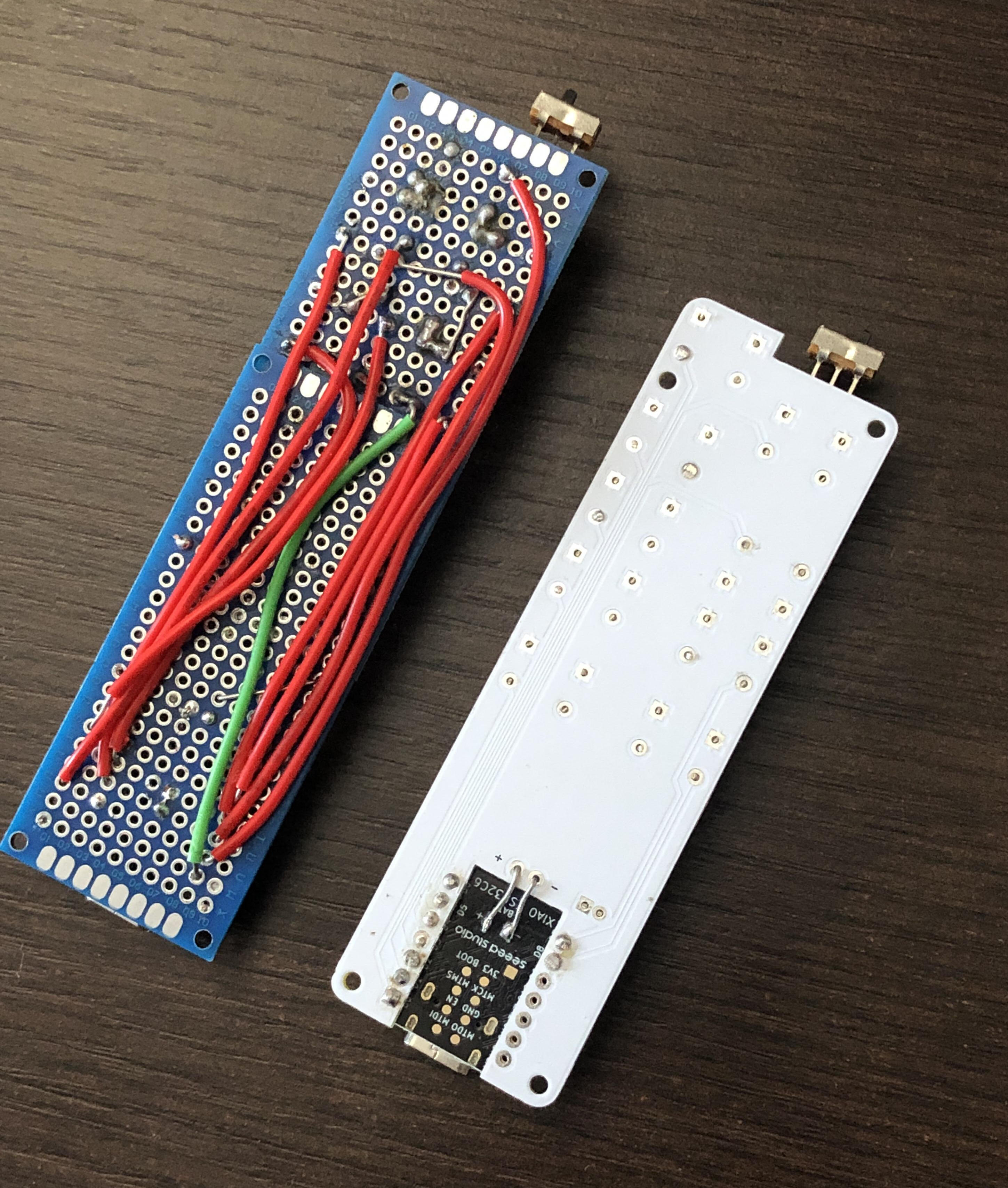
Over the past few weeks I’ve learned how to use KiCad and designed my first PCB with the goal of replacing the perfboard to make the assembly cleaner and the remote more compact. I just received the PCB so I can now go ahead with the integration.
Updating the 3D model and choosing the buttons
From the previous prototypes I had already developed a 3D model of the enclosure. When designing the PCB, I updated that model to accommodate it and included a mock of the PCB using dimensions taken directly from KiCad once the design had become reasonably stable. After that I continuously adjusted the model to match later revisions.
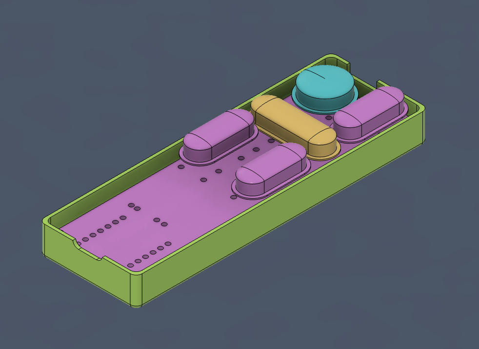
The first objective before soldering the PCB is to decide which switches to install. I have a collection of very common 6×6 mm tactile switches with various stem heights. The stem height is closely related to the final thickness of the remote, so choosing the right one is important. To determine the ideal stem height, I use the 3D model I prepared.
Before going in I take a few measurements to verify the model and adjust it if necessary. I confirm that the PCB is indeed 1.6 mm thick as expected. With the ESP32 installed, the total height is about 6 mm, and with the battery it reaches roughly 7 mm. Since the body of the switches is 4.7 mm high, the battery appears to be the component that determines the minimum enclosure thickness. I update the model accordingly.
Before calculating the required button dimensions, I try to reduce the overall thickness as much as possible. The enclosure of the first prototype was 19 mm thick, and for this new version I’d like to see how thin I can make it. At the very beginning of the project, I built a mock-up to determine the ideal shape and concluded that 10 mm would be a good target thickness. That seems ambitious, but I am curious to see if I eventually achieve it.
One factor that affects the total thickness is the space left between the bottom of the enclosure and the PCB. I therefore try to minimize anything protruding beneath the PCB. I determine that I can solder the switches from the top side rather than from the bottom as originally planned. If I then trim the leads, there will be no protrusion underneath the PCB in the switch area. The same applies to the battery connector. The ESP, however, requires solder joints on the underside and there will also be two battery wires connected from below. I had originally planned for 2 mm of clearance beneath the PCB, but with these considerations I estimate that 1 mm should probably be ok.
The enclosure consists of two parts, a top half and a bottom half. Until now, the shell thickness was 2 mm. That seemed like a reasonable minimum to ensure rigidity, but I want to try reducing it to 1 mm. With all these changes, I end up very close to my 10 mm target thickness. I am surprised and excited.
With the model updated, I can return to the button calculations. I determine that a stem height resulting in a total height of 8 mm measured from the underside of the PCB would be ideal. In my collection, the closest options are either slightly shorter or slightly taller. In my design the stem guides the button caps that cover the switches, and I’m concerned that the caps won’t be properly guided if the switch is too short. I can always accommodate a slightly taller switch by adjusting the cap design, but the opposite seems more problematic. I therefore choose the taller option.
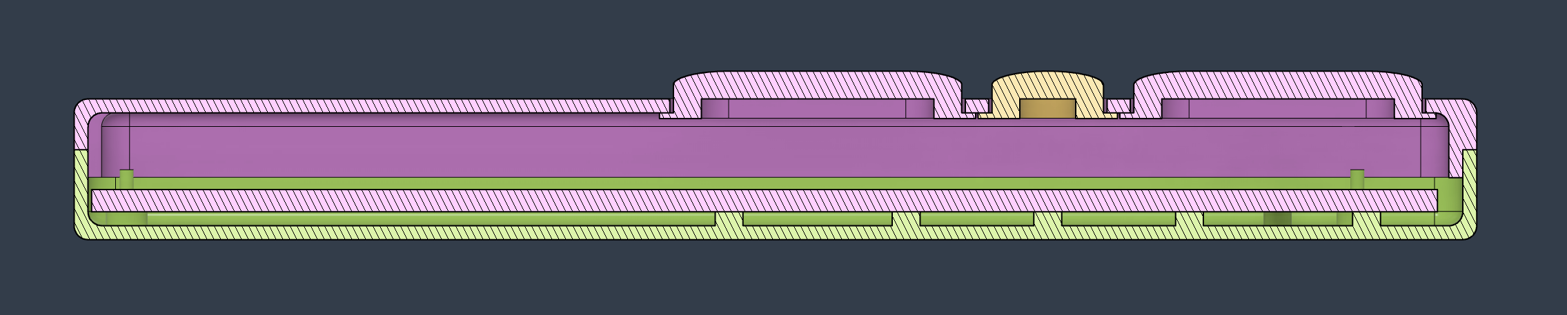
In the end, I spent a good part of an evening thinking about dimensions, measuring components, adjusting the model, and selecting the switches. It feels like I spent far more time than necessary. I think I was having trouble visualizing how all the dimensions interacted with one another. I chose to place the enclosure seam at the midpoint of the USB port, so most calculations were referenced more or less from that point, and I think that confused me somehow. I may also have been worried about choosing the wrong switches and having to redo the soldering, even though that wouldn’t have been a major issue. Or perhaps I was simply tired.
In any case, I stuck with it and eventually arrived at a design I was satisfied with, and I felt ready to start soldering the next day.
Preparing for soldering
Before getting started, I think about the order in which the components should be soldered. The on/off switch will require holding the PCB in a vise or helping hands, and that’s easier to do before anything else is mounted. It will therefore be soldered first. Next, the battery connector is located close to the ESP32, so if I solder it from the top side it will be easier to do before the ESP32 is installed. After that I can solder the buttons and finish with the ESP32.
While examining the PCB, I suddenly become doubtful and check the schematic to verify which ESP pins I used. I then consult the official documentation to make sure they are suitable for my use case. Everything looks good.
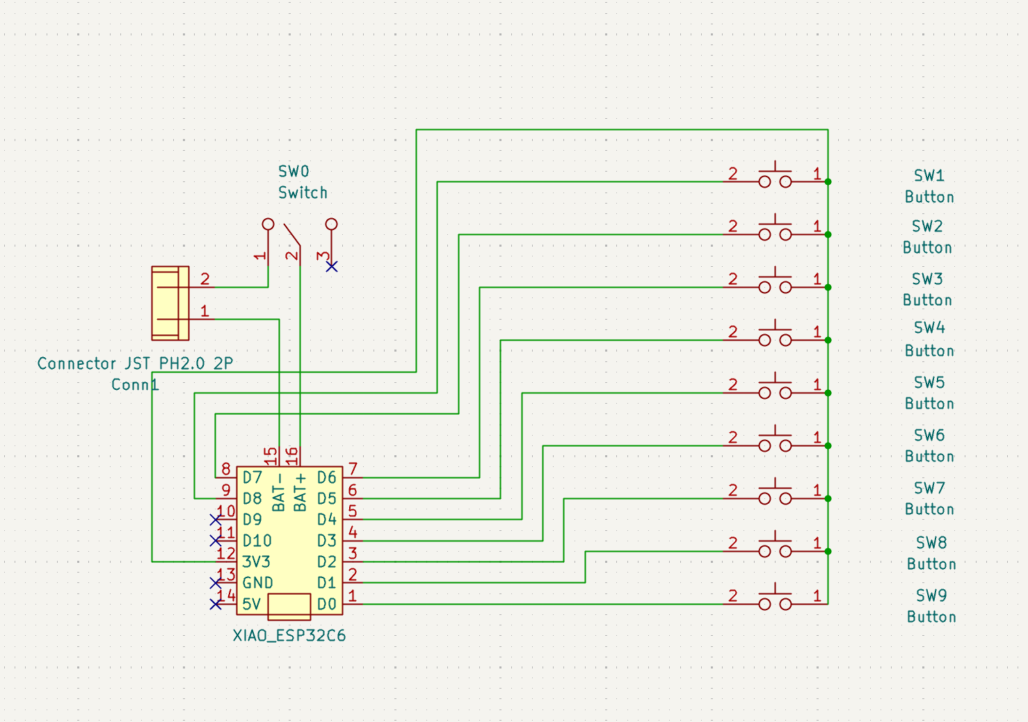
While I’m at it, I update the Arduino code because the button-to-pin mapping has changed compared to the previous prototype. I also take the opportunity to restructure the code a little and add comments. The labels I added to the PCB make it easy to identify which function corresponds to which pin, whereas on previous prototypes I always ended up manually testing the buttons after the fact to find out which is which.
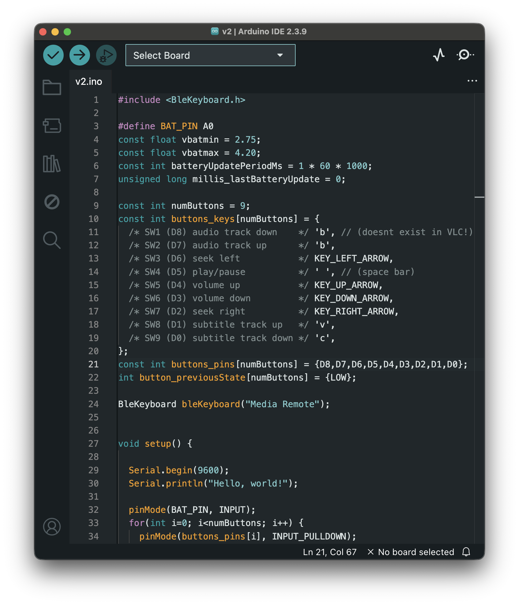
The code is available on GitHub.
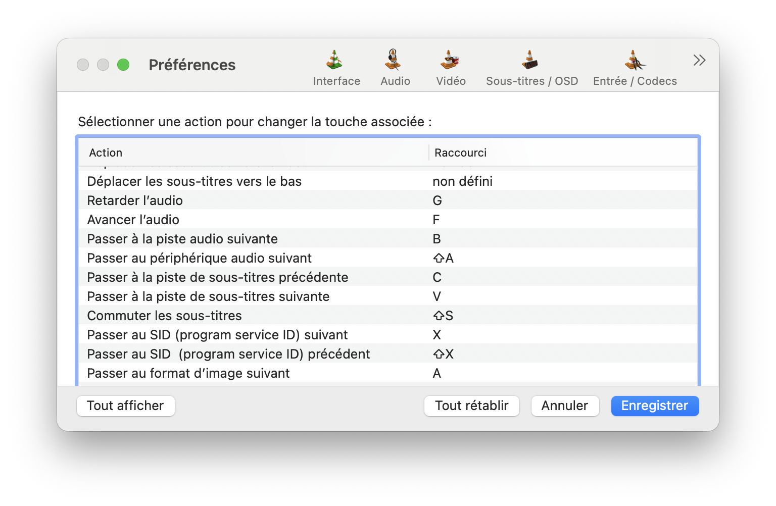
Compared to the previous prototype, I added a button to cycle through audio tracks in both directions so that the audio controls would mirror the subtitle controls. However, when I looked up the VLC keyboard shortcut, I discovered that there doesn’t seem to be a shortcut for switching to the previous audio track. Surprisingly enough.
I therefore decided that both buttons would simply switch to the next audio track 🤷♂️
Soldering
I’m still a beginner when it comes to soldering, but I’m making progress. Ever since I got my FNIRSI DWS-200 soldering station with an F210 tip, things have generally gone quite smoothly. I systematically apply a little flux before each joint, put some solder on the iron, and let the molten metal flow into place by itself. Overall, I’m quite proud of my solder joints.
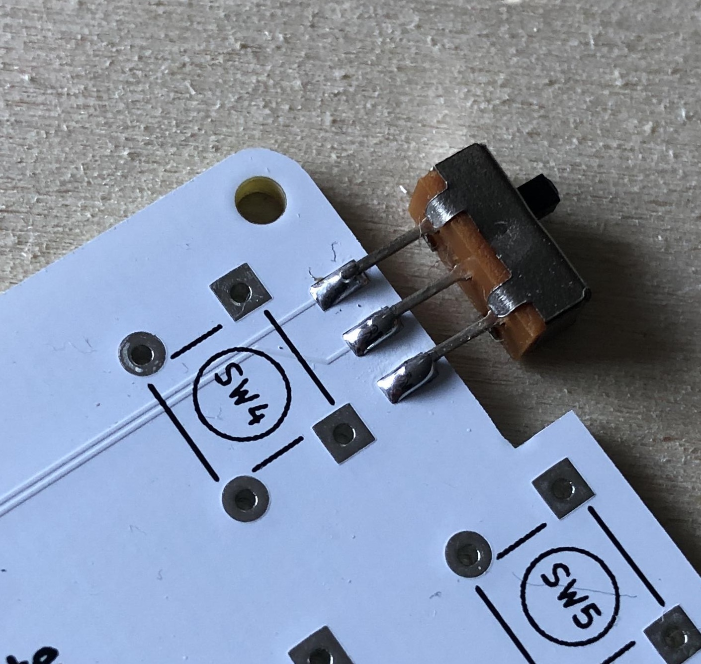
Soldering the battery connector from the top side didn’t present any particular difficulty.
For the ESP32, I designed holes on the PCB aligned with the holes on the ESP board. The idea is to pass a piece of wire through each hole and solder it on both sides. I experimented with a technique that consists of weaving a single wire through all the holes, alternating between top and bottom like a sewing thread. Looking back, it probably wasn’t the best approach. Nevertheless, the final result looks clean.
I had initially planned to solder every pin, but then I remembered that most of them aren’t actually used. I therefore soldered only the nine pins required by the buttons.
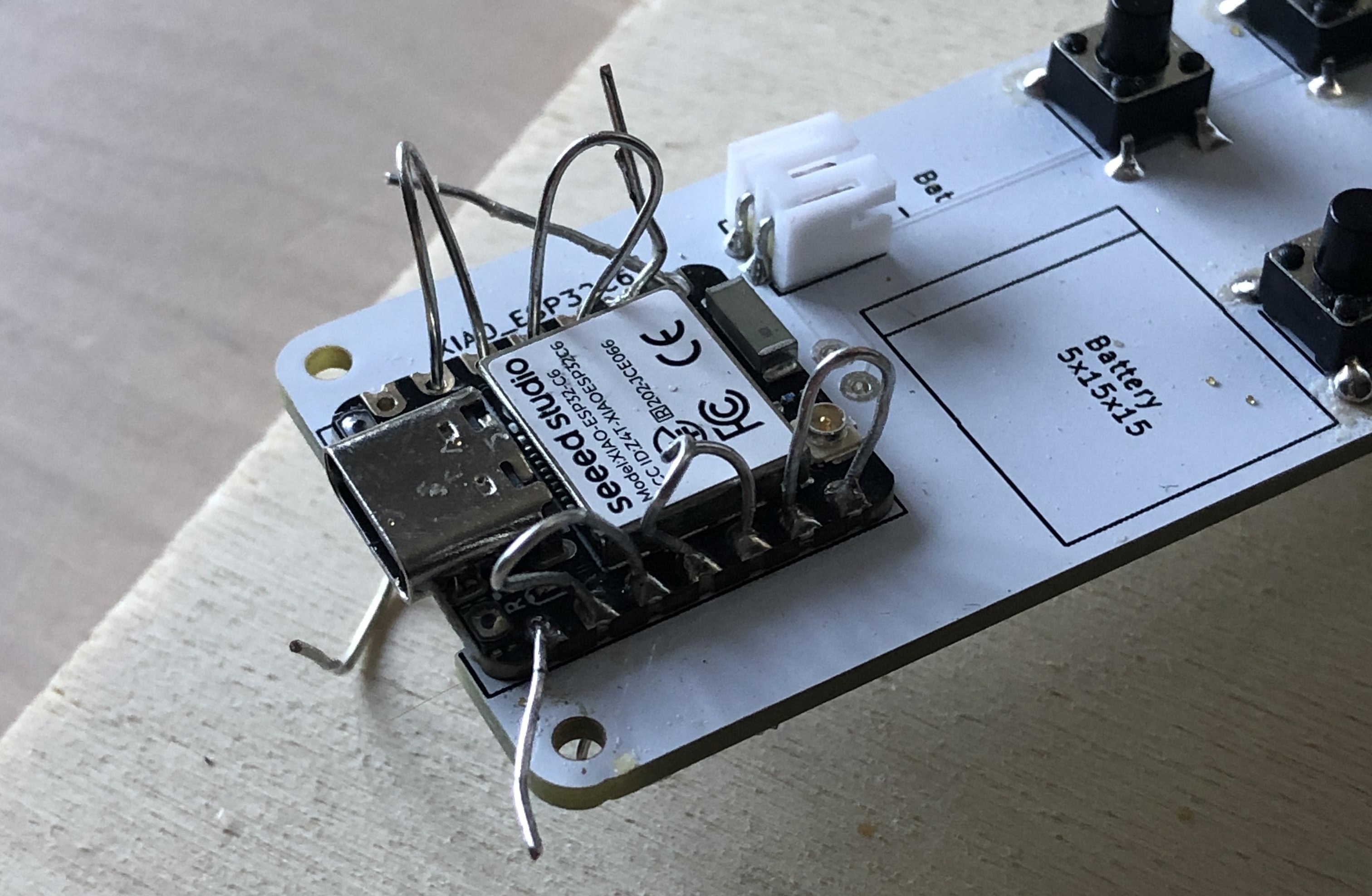
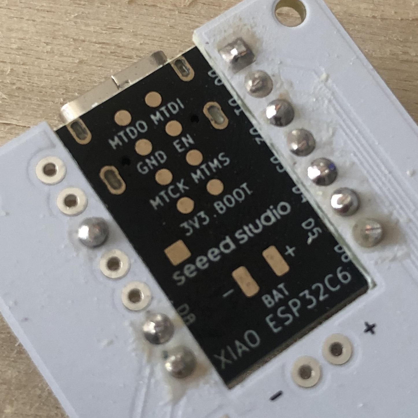
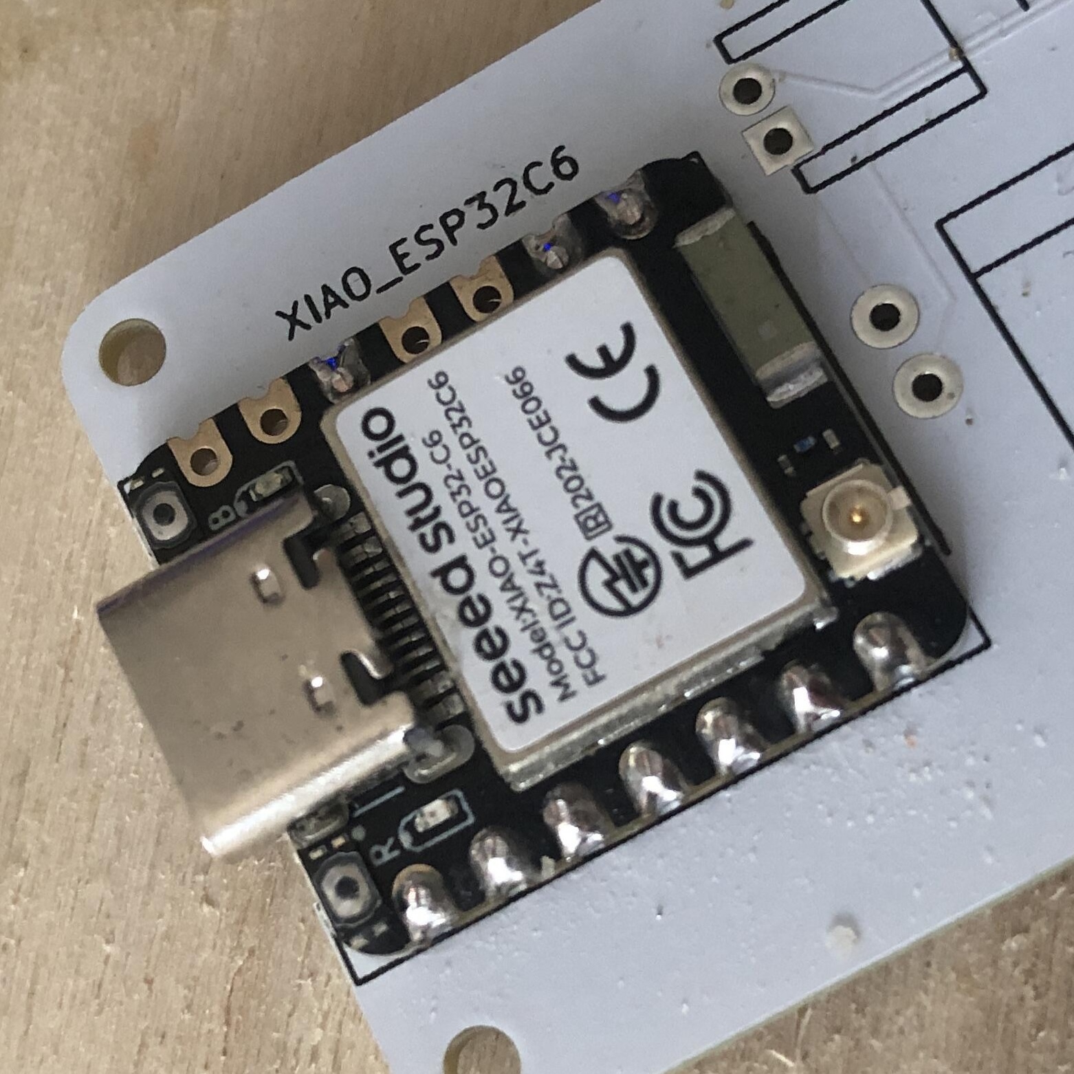
The final solder joints connect the battery pads located underneath the ESP32 to the connection points provided on the PCB. To do this, I pass a wire through a PCB hole and solder its end directly onto the ESP pad. After that, I trim the switch leads and the battery connector leads, and the board is finished. Soldering requires quite a bit of precision and sustained focus, and by the end I can feel it in my back.
First tests
With the board completed, I decide to test it. This is the moment of truth. I flash the firmware, Bluetooth connects successfully, and I begin testing the buttons.
Initially, none of the buttons work. I think about it for a moment. When a button is pressed, it is supposed to connect 3.3 V to one of the ESP32 pins. I then realize that I forgot to solder the ESP32’s 3.3 V pin. I used a power plane to distribute 3.3 V to the buttons, so there is no obvious visible trace connecting it to the ESP itself. That’s probably why, when I decided not to solder all the pins, I accidentally skipped that one. I check that I haven’t forgotten any other connections, fix the issue, and the buttons immediately start working.
Now the button for switching to the previous subtitle track doesn’t work. It’s supposed to send the C key. I test it in a text editor and indeed nothing is sent. I check the code, but nothing stands out. I inspect the solder joints; same thing. I manually apply 3.3 V directly to the corresponding ESP32 pin, bypassing the button, and still nothing happens. The same test on the neighboring pin successfully triggers its associated key press. That suggests a software problem. I dive back into the code and remember that earlier versions used pin A0 to read the battery voltage. I no longer use that feature here, but it’s probably still interfering somehow. I decide to remove all battery-monitoring code entirely, since my PCB design wouldn’t support such features anyway. That solves the problem.
Finally, the button used to navigate audio tracks behaves incorrectly. It always sends the key twice. The two buttons are connected to adjacent pins, and after inspecting the connections more closely, I think I can see a tiny solder bridge between them. I clean it up, and the issue disappears.
Connecting the battery
I then try connecting the battery using the dedicated connector. I’m happy that I implemented a proper connector this time, because on all previous prototypes I had improvised makeshift battery connections using two loose wires. This actual connector looks much cleaner.
Shortly after plugging in the battery, I hear crackling noises. I immediately disconnect it, and for a moment I’m worried that the battery might catch fire or explode. The on/off switch is in the OFF position, so in theory the battery shouldn’t have been connected to the ESP32. The ESP32 itself feels slightly warm, which doesn’t do much to reassure me.
While inspecting the battery connector solder joints, I think I can see a connection between the two pads. I quickly clean it up and take the opportunity to remove the flux residue left on the rest of the board while also giving all the solder joints a quick inspection. I reconnect the ESP32 to my computer and everything works normally. That’s reassuring.
I reconnect the battery and hear crackling again. This time I grab a multimeter and confirm that there is still a short circuit between the battery connector terminals. It’s really the worst possible place to work on because it’s right next to the ESP32 and not particularly accessible. These were among the first solder joints I made that day, and honestly they could have been better. The PCB pads are very close together, and I used quite a lot of solder. I remove some of it with a desoldering pump, and things immediately look cleaner. I check again with the multimeter and everything looks good. Now I just hope the battery hasn’t been damaged.
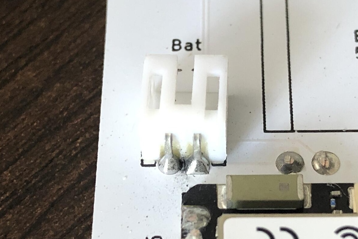
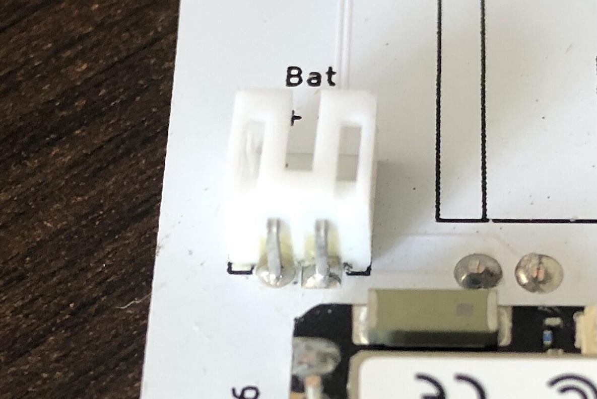
I reconnect the battery while listening carefully, and everything seems fine. Finally. I flip the power switch on and the remote works perfectly.
In the end, there were quite a few issues after soldering, but nothing serious (for now). Everything was resolved quickly, and I can now move on to the enclosure.
Printing the enclosure
Before printing the enclosure, I still need to adjust the opening for the on/off switch. I deliberately waited until after soldering it to take the final measurements because, unlike the buttons, it doesn’t have a completely fixed mounting position. I designed rectangular pads that allow its leads to be soldered parallel to the PCB, meaning its exact position is partially determined during assembly. The lateral positioning matches the theoretical position nicely. While I’m at it, I reduce the clearance slightly to bring the enclosure as close to the switch as possible.
I also add fillets to the inner corners to improve strength. Reducing the wall thickness created a stress concentration area near the corners because of the external rounding.
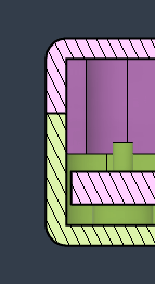
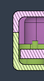
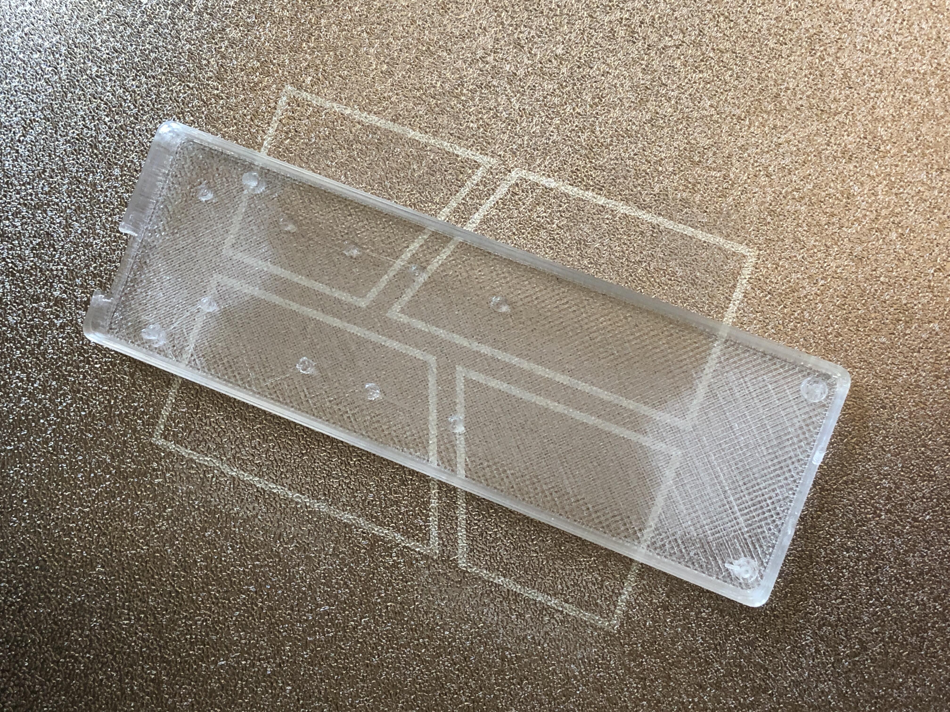
Since the design is still experimental, I print one part at a time instead of printing everything at once. That way I can validate each piece as I go and make adjustments if necessary. I use transparent filament so that I can see how the components fit inside the enclosure.
Repairing the battery connector
While working in Fusion to prepare the enclosure prints, I had left the PCB beside me with the battery connected and at some point I heard crackling again. This time, before I had time to disconnect it I actually saw sparks. I worried about the battery, but it showed no signs of damage and wasn’t even warm. The ESP32, however, felt slightly warm, which concerned me.
While the enclosure is printing I inspect the battery connector again and I notice black marks this time. I clean everything and use the desoldering pump once more. The connector pin spacing is only 2 mm, which isn’t much. I deliberately used smaller-than-normal pads to prevent them from touching, but perhaps they’re still too close together. After cleaning, I reconnect the battery. Initially everything seems fine, but when I wiggle the connector slightly, smoke appears. Not good.
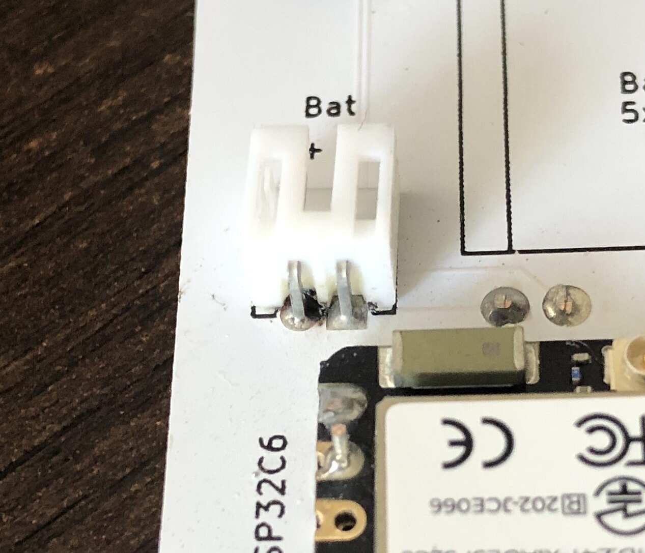
The connector blocks the view of part of the solder joints, and there may be defects I can’t see. I therefore decide to desolder it completely. I’m glad I hadn’t put away the soldering equipment yet. I struggle a bit to remove the connector, but eventually succeed. Unfortunately, one of the pads lifts from the back side of the PCB. For a moment I consider abandoning the connector and going back to simple wires like on the previous prototypes. But in the end I decide to give the connector another chance. This time I solder it from the underside wherever possible despite the damaged pad. I solder the intact pad from below and the other one from above. In the confusion, I accidentally solder the same pad from both sides. This time I try to use as little solder as possible.
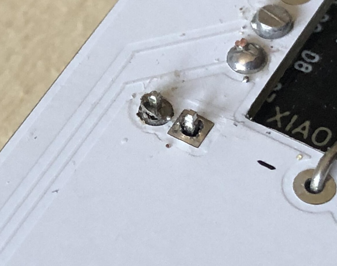
I check with the multimeter to make sure there are no shorts, and I also verify continuity with the rest of the circuit. Everything appears to be fine. I wiggle the connector and test repeatedly and it seems to be holding. I consider adding a drop of liquid glue to stabilize the connection. If I do that and need to rework it again, things will start becoming delicate. I decide to go for it anyway.
Integration into the enclosure
The lower half of the enclosure has finished printing. I was worried that a bottom thickness of only 1 mm would be too fragile, but it actually feels quite solid. I install the PCB inside, and it fits perfectly. The transparent enclosure allows me to verify that the PCB is correctly resting on all the support points I designed into the model, which is nice. Everything looks good, so I start printing the upper half.
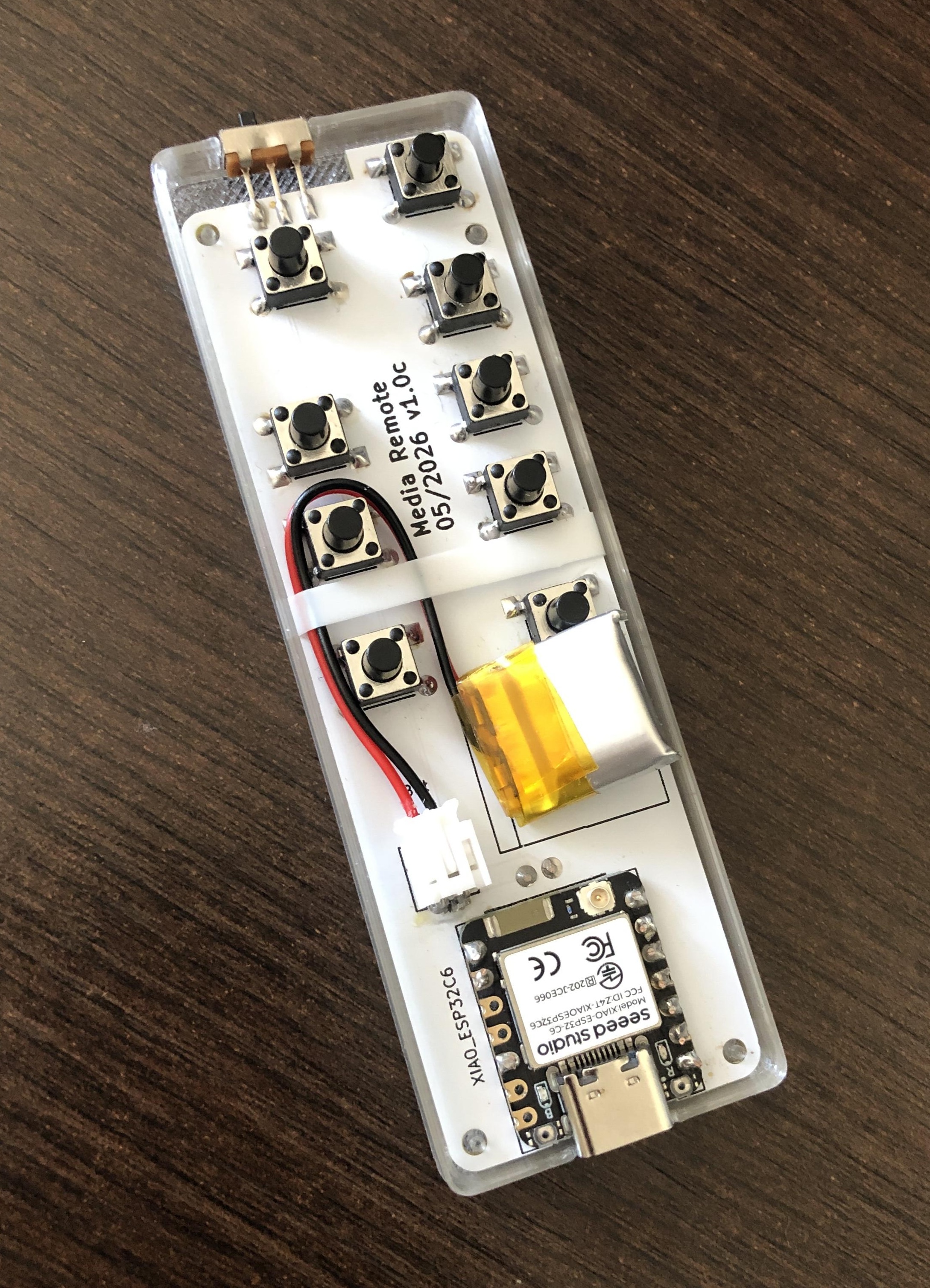
Once printed, I assemble the upper half of the enclosure, but something prevents it from closing completely. It turns out to be the battery connector. Of course it is, my nemesis of the day. I realize that I never included it in the thickness calculations I made at the beginning of the project. In theory, it should fit because it is only 6 mm tall, but after all the adventures of the day it ended up being soldered slightly higher than intended. Despite that the enclosure is remarkably thin overall and I really like the result.
I print a button cap and test it, only to discover that it prevents the enclosure from closing. I’m off by nearly 2 mm. That means it’s time to adjust the button caps. I note that future revisions could easily use shorter switches, but definitely not taller ones.
Unexpected loss of the ESP
While the upper half of the enclosure was printing, I continued testing the system. The Bluetooth connection would occasionally drop whenever I moved the battery around, indicating that the board was momentarily losing power. That’s probably preferable to a short circuit, but it’s still not ideal. As long as I didn’t touch anything it seemed stable enough.
Then suddenly everything stopped working. At first I suspected that the battery had gone flat, so I tried charging it. I wasn’t particularly eager to connect the board to my computer because I was worried about what a possible short circuit might do to it, even though the actual risk was probably low. Instead, I plugged it into the wall, and it worked. I disconnected it to inspect the connections with a multimeter. Everything seemed fine. I plugged it back into the wall. It worked for a few moments, and then once again the Bluetooth connection disappeared even though the board was still powered by USB. That felt like a very bad sign.
I disconnected everything, unplugged the battery, and connected the board to my computer. Arduino IDE no longer detected it.
I noticed that the ESP felt warm, and that immediately reminded me of a previous prototype that had died in a similar fashion. I checked it with a multimeter and the pin that normally outputs 3.3 V was dead, whereas on a working ESP board, I could clearly measure 3.3 V there.
At that point I started questioning myself. This was the second prototype that had failed in the same manner. I began wondering whether I was doing something that ESP boards simply don’t tolerate. Something related to the battery or power circuitry. Of course the shorts in the battery connector might have had something to do with the failure of this board, but it probably wasn’t the whole story.
While I was working on the enclosure I also spent some time discussing the issue with ChatGPT. I mostly use it as a thinking tool and an idea generator. I try to describe the problem and the sequence of events as clearly as possible. Then I read its suggestions and see whether any of them resonate with me. I reply with whatever thoughts come to mind and use the conversation to drive my thinking forward.
I still find phrases such as “A failure mode I’ve personally seen on small ESP32 boards” rather surprising. I feel like this kind of wording has become increasingly common recently, and I think AI agents should not talk that way. Although like everything AI, it could be the topic of an interesting philosophical discussion. Anyway.
The main hypothesis was that the power circuitry had failed, but I already suspected that. Among the things the AI suggested was “The fact that one board works and others don’t suggests a process-related issue rather than a design issue. Solder bridges or conductive debris under the board.” That points toward assembly mistakes or accidental damage during handling. It also mentioned electrostatic discharge as a possible cause. Perhaps I should be more careful when handling the boards.
Another comment that caught my attention was “The battery pads are tiny and located near sensitive circuitry.” The battery pads have always made me a little uncomfortable. They are small, and I don’t find them particularly convenient to solder to. I’ve indeed always been worried about damaging the board while heating those pads with the iron.
ChatGPT pointed out that my design directly connects 3.3 V to GPIO pins through the buttons, wich can potentially be dangerous if a GPIO is accidentally configured as an output and driven low. It suggested: “Adding a 1 kΩ–10 kΩ series resistor between each button and the GPIO is cheap insurance.” I found that suggestion interesting and made a mental note of it.
I did some research to see how people use ESP boards with a battery and how they connect it to the pads underneath the ESP module, but nothing stood out. I also looked into common techniques for board-to-board connections using this type of pad arrangement. The most accessible method I found was to place a via directly in front of the pad and let solder wick into it. I was quite skeptical of that approach.
I continued discussing the issue with ChatGPT, and at one point it mentioned: “The XIAO battery pads are intended for a LiPo connected all the time. Power transients from hot-plugging batteries can stress or even kill the regulator.” That observation aligned surprisingly well with what I had experienced. In all the examples I had seen, people soldered the battery directly to the pads. I don’t particularly like the idea of a board being permanently powered, which is precisely why I added an on/off switch in series with the battery. However, ChatGPT pointed out that repeatedly connecting and disconnecting the battery—especially while USB power is also connected—can place significant stress on the power-management circuitry and eventually cause it to fail.
I like robust systems. In this case, I had been connecting and disconnecting USB, plugging and unplugging the battery, and generally experimenting without taking any special precautions because I expect—or rather hope—that the system tolerates this sort of use. Recent events suggest that it might not.
This isn’t a definitive conclusion though because the previous prototype, which I still use regularly, continues to work fine despite the fact that I often disconnect the battery using its power switch several times during a movie because the battery life isn’t great. Perhaps the real problem only occurs when USB power is connected at the same time.
In any case, from that moment onward I decided that future versions of my remote (and other projects for that matter) would have the battery connected directly to the ESP32, and I would rely on the ESP’s sleep modes to preserve battery life instead of physically disconnecting the battery.
Second Board and finalizing the enclosure
The PCB manufacturer supplied me with about ten boards, so I have plenty of room for mistakes and experimentation. I also have multiple copies of all the components, so that’s not an issue either. I still have two spare ESP32 boards available. The only components I have in limited quantities are the tactile switches. I only have ten of each stem-height variant, but I can always adapt my design to it.
I therefore decide to assemble a second PCB while leaving out everything related to the battery. My goal is simply to determine whether the system remains reliable without any battery circuitry involved. If it does, I’ll reconnect the battery later but replace the power switch with a simple wire.
So it’s time for another soldering session. At least it’s an opportunity to practice. My technique continues to improve. This time I only need to solder the switches and the ESP32 connections, so the work goes quickly. I also make a conscious effort to touch the ESP board as little as possible with my fingers.
Once assembled, I test the board. Everything works perfectly on the first try. I leave it connected via USB while continuing to work on the enclosure and periodically verify that it is still functioning. I also try to avoid unplugging and reconnecting it unnecessarily.
I revisit the button cap I printed earlier and decide to increase its internal height by 1 mm without changing its external height. Unfortunately, the cap now rests directly on the switch body, making it impossible to click. So I go back to the measurements and realize that, in the current design, there is barely 1 mm of clearance between the switch body and the enclosure, which is very little.
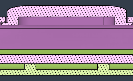
I decide to increase the enclosure height by 1 mm. That won’t significantly affect the overall thickness, but it will provide some additional clearance for the buttons. This time the enclosure closes properly and the buttons work, but they barely protrude from the surface. I therefore increase the cap height by another millimeter by modifying a dimension in the CAD model. Unfortunately, I don’t notice that this change also increases the internal height of the cap. As a result the button no longer clicks. I fix the model and print yet another cap. I feel the process is more laborious than it needs to be. By this point it’s late in the day and my concentration is fading. Losing the ESP board earlier hasn’t helped my morale either.
The button-cap mechanism doesn’t feel ideal to me, and I may revisit it in the future. In reality, the biggest issue is that now that the remote has become dramatically thinner, the switch bodies themselves are starting to feel oversized. I make a note to look for thinner switches, assuming such components exist.
Closing thoughts
I end the day feeling tired and somewhat discouraged. The exact reason why the ESP boards failed remains unclear, and that leaves me with the impression that the system as a whole is fragile—that the board could die at any moment because of some seemingly harmless action. I really don’t like that feeling. The enclosure and the buttons also leave me with mixed impressions. On one hand, the whole thing feels flimsy. On the other hand, there are still friction points.
Overall, I’m not particularly happy with the result, but I think that’s mostly the fatigue and frustrations of the day talking. I try to take a more objective look at what was actually accomplished. I successfully validated that the PCB works and that I can reliably solder components onto it. The PCB allowed me to significantly refine the overall design of the remote control, which was the primary goal of this iteration. That’s undeniably positive.
All the remaining issues appear solvable. For the ESP, even though the exact cause of the failures is still unclear, I will connect the battery directly and be more careful when manipulating the board. For the enclosure and buttons, I can explore ways of joining the two halves together, perhaps using screws or magnets. As for the buttons, I’ve already identified some ultra-low-profile switches that could improve the mechanism.
I have a stockpile of PCBs available, which means I can afford to experiment with the mechanical aspects of the design. I’d love to find a way to connect and disconnect the ESP32 board from the PCB without having to solder it every time. That would be ideal. In the future, I could design a dedicated breakout board and connect it to the main PCB using a flat connector. There are plenty of possibilities and thinking about this makes me excited again.
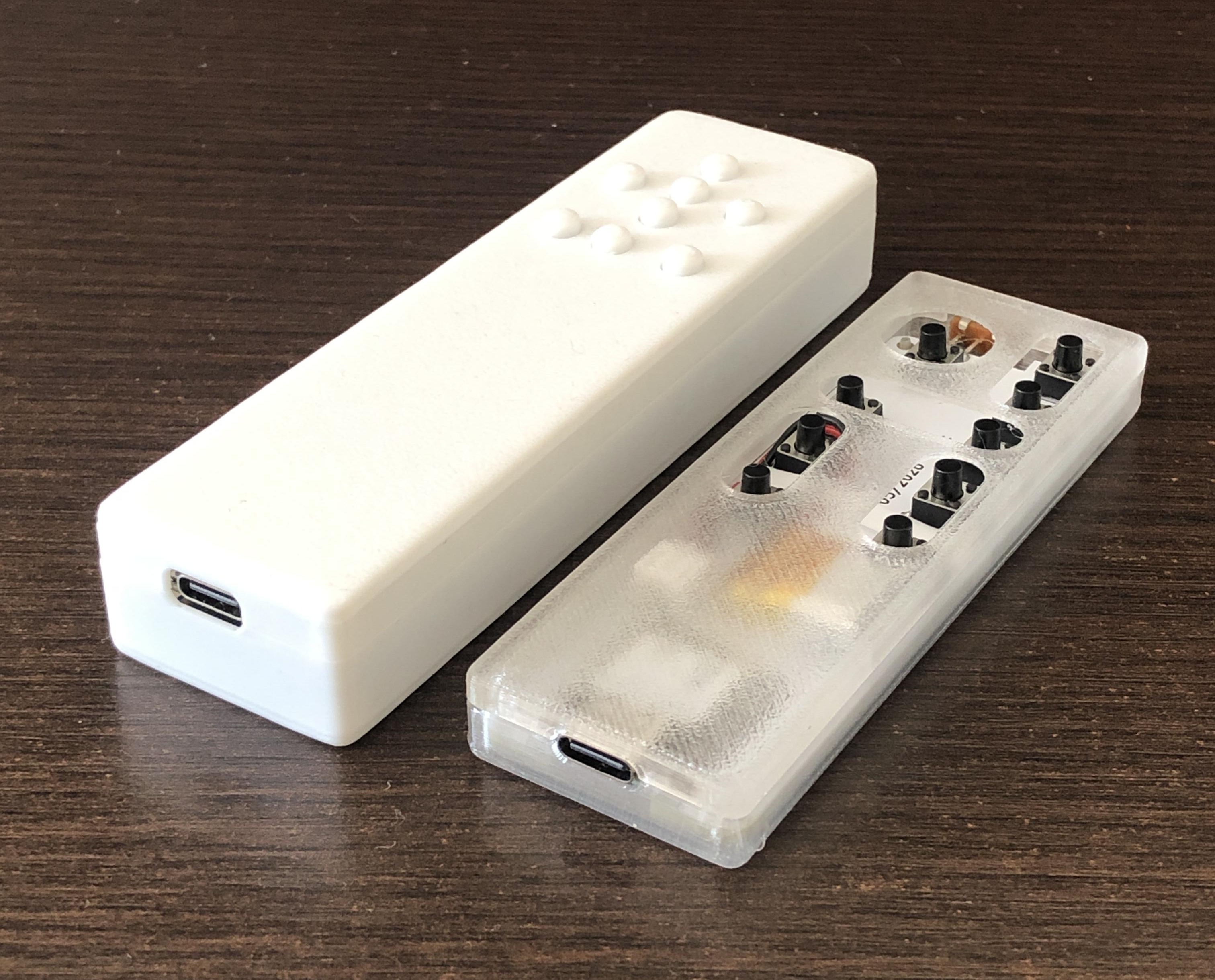
But the final conclusion of the day is that the project has transitioned from a prototyping / proof-of-concept phase into a phase of iterative refinement.
Up until now, the goal was simply to create something that worked according to the intended requirements: a wireless remote control that could be comfortably held in the hand. Functionality was the priority, while aesthetics and construction quality came second. I didn’t pay much attention to user comfort, I used overly generous tolerances to ensure things would fit, and so on.
Now that the core functionality has been established, my focus has shifted toward making the design clean and elegant. I want things to be precise, minimal, and robust. That requires accurate calculations, balancing competing constraints, iterating through small variations, and carefully documenting what works and what doesn’t.
I hadn’t fully realized this shift in objectives. I simply continued working the way I had so far. But I now understand that I’ve reached the limits of that original approach. The project is ready for its next phase, and the development process needs to evolve accordingly.
What’s next
I’m going to use the new battery-less version for a while and see whether it survives. If it does, I’ll reconnect the battery without a power switch and start investigating the ESP32’s sleep modes.
At the same time I’ll continue exploring improvements to the enclosure and the button mechanism. I already have several ideas for joining the two enclosure halves together. I want the design to remain serviceable and easy to disassemble, so glue is out of the question. I’ve already ordered the ultra-low-profile switches that should allow for a more robust button mechanism, assuming I can solder them onto the existing PCB.
As I work through these improvements, I’ll also formalize the project more thoroughly by creating a proper design log containing notes, diagrams and equations describing the relationships between parameters, comparison tables for alternative solutions, and so on—similar to what I’ve done for some of my other projects.
I use generative AI to write and/or translate the content featured on this website. AI serves only as a tool for productivity and inspiration, I make sure that the final texts always reflect my personal voice and style.